Table - table 1-12: ports – Achronix Speedster22i User Macro Guide User Manual
Page 27
I/O Cells
IOPAD_D2
Speedster Macro Cell Library
PAGE 10
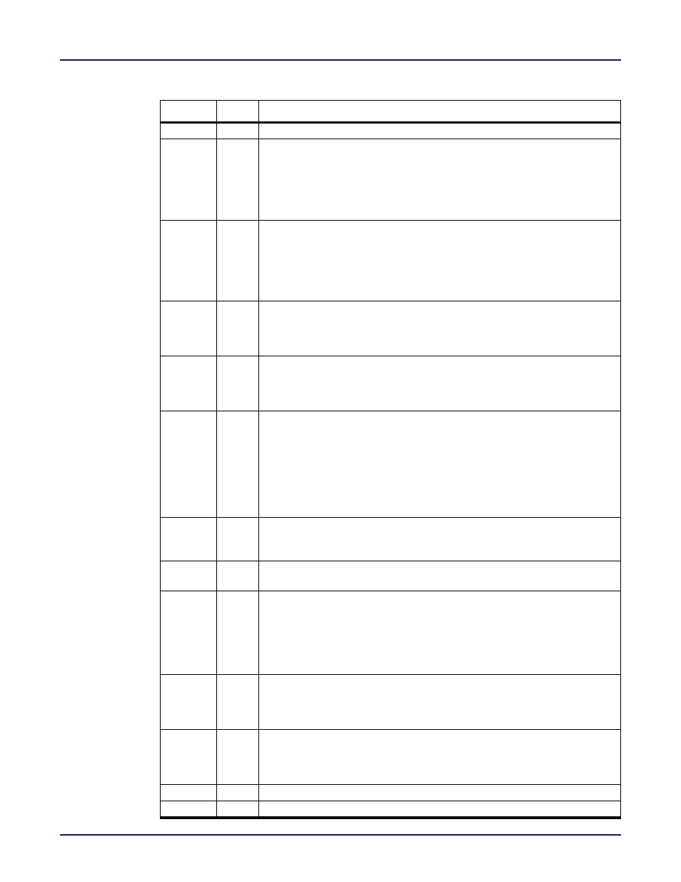
Table 1-12: Ports
Name
Type
Description
pad
inout
Bidirectional device pad.
dina
input
Positive-edge based data input. Data is clocked into the dina register upon
the rising edge of the txclk input when the txdata_en signal is high. It is
routed to the pad on the following rising edge of the clock. If the oe input
was high during the same clock period of the dina input, the pad will be
actively driven with the dina data during the portion of the clock period
when txclk is high.
dinb
input
Negative-edge based data input. Data is clocked into the dinb register
upon the falling edge of the txclk input when the txdata_en signal is high. It
is routed to the pad on the following rising edge of the clock. If the oe input
was high during the same clock period of the dinb input, the pad will be
actively driven with the dinb data during the portion of the clock period
when txclk is low.
douta
output
Positive-edge based data output. Data is clocked from the pad to an inter-
nal register on the rising edge of the clock. On the next rising edge of the
clock, if the rxdata_en input is high, the data will appear on the douta out-
put.
doutb
output
Negative-edge based data output. Data is clocked from the pad to an
internal register on the falling edge of the clock. On the next rising edge of
the clock, if the rxdata_en input is high, the data will appear on the doutb
output.
oe
input
Output Enable (active-high).The output enable input must be aligned with
the dina and dinb inputs. The oe data is clocked into the oe register upon the
rising edge of the txclk input when the txdata_en signal is high. It is routed to
the enable of the pad on the following rising edge of the clock. The value of
oe is applied to the interval of both the dina and dinb data at the pad. A high
value on the oe input results in the dina and dinb data being driven onto the
pad. If the value of oe at the enable intput of the pad driver is low, the pad
will be placed in a high-impedance state.
txdata_en
input
Transmit Data Enable (active-high). A high value on txdata_en enables the
dina, dinb, and oe inputs to be clocked into the transmit and output enable
registers.
rxdata_en
input
Receive Data Enable (active-high). A high value on rxdata_en enables the
received data to be clocked into the douta and doutb output registers.
txrstn
input
Output Register Asynchronous Reset input. A low value on txrstn per-
forms an asynchronous initialization of the Output Register if the rstmode
parameter is set to “async”. The value initialized into the Output Register is
determined by the value of the rstvalue parameter. A low value on txrstn also
asynchronously initializes the output enable register to a low value indepen-
dent of the value of the rstmode parameter.
rxrstn
input
Input Register Asynchronous Reset input. A low value on rxrstn performs
an asynchronous initialization of the Input Register if the rstmode parameter
is set to “async”. The value initialized into the Input Register is determined by
the value of the rstvalue parameter.
srstn
input
Synchronous Reset Input. A low value on srstn performs a synchronous ini-
tialization of the input registers and output registers if the rstmode parame-
ter is set to "sync". Setting the rstmode parameter to "async" disables the
synchronous reset.
txclk
input
Output Register Clock Input.
rxclk
input
Input Register Clock Input.