Heading3 - advanced mode fifo reset operation, Advanced mode fifo reset operation – Achronix Speedster22i User Macro Guide User Manual
Page 156
Memories
BRAM80KFIFO
Speedster22i Macro Cell Library
PAGE 139
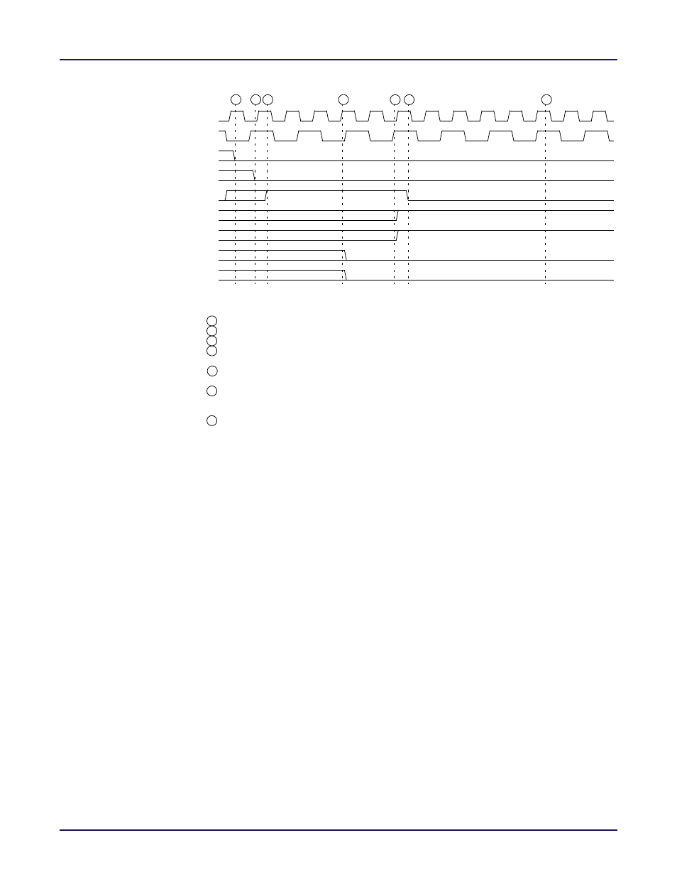
Figure 6-12: Basic Mode FIFO Reset Timing Diagram
Advanced Mode FIFO Reset Operation
The FIFO provides the user with several options to reset the FIFO from either the read or write
clock domains. The reset operation may either be sychronous with respect to the read and/or
write clock domains or the user may enable the internal reset synchronization circuitry to
synchronize the reset inputs. The capability for synchronous resets is provided to allow the
user the fastest response between the reset operation and when the FIFO is ready to be
written. Internal to the FPGA, the read and write pointers have synchronous reset inputs.
The FIFO macro provides the necessary circuitry to perform the synchronization of the
pointer resets without the need to implement synchronization circuitry within the FPGA
fabric.
The Write Pointer reset circuitry is configured via the wrrst_sync_mode and
wrsrt_sync_stages parameters and the Read Pointer reset circuitry is configured via the,
rdrst_sync_mode and rdrst_sync_stages parameters. The reset operation of the read and write
pointers is configured independently so that in addition to configuring the reset to be
synchronous or synchonized, the resets can also be configured to respond to one or both of the
wrrst or rdrst input signals. This independent configuration additionally allows the wrrst and
rdrst inputs to operate separately on the write and read pointers so that the FIFO may be used
as a building block for finite state machines or allow the read pointer to be reset for re‐read
operations.
The user must take care to make sure the resets are synchronized to the proper clock domain.
If the Read Pointer or Write Pointer synchonizers are bypassed, synchronization of the rdrst
and wrrst will have to be performed within the FPGA fabric unless the user is already
providing resets that are synchronous with the appropriate clock domain.
wrclk
rdclk
wrrst, rdrst
empty
almost_empty
full
almost_full
wren
rden
1. User reset signal connected to wrrst and rdrst inputs
Note: This timing diagram assumes:
2. wrrst and rdrst configured as active-high wrrst_rstval = 1’b1, rdrst_rstval = 1’b1.
A
B C
Event : The empty and almost_empty flags are asserted (wrrst_sync_stages + 2) active rdclk edges after
Event : The user (wrrst and rdrst) reset signals are deasserted after a minimum of:
E
F
the reset inputs are asserted.
D
G
Event : The user (wrrst and rdrst) reset signals asserted.
C
Event : The full and almost_full flags are deasserted (rdrst_sync_stages + 2) active wrclk edges after the
D
reset inputs are asserted.
max{(wrrst_sync_stages + 3) rdclk cycles, (rdrst_sync_stages + 3) wrclk cycles}
Event : The first FIFO write operation may begin:
max{(wrrst_sync_stages + 3) rdclk cycles, (rdrst_sync_stages + 3) wrclk cycles}
after the user (wrrst and rdrst) reset signals are deasserted.
G
E F
Event : The user must disable the wren signal during the reset operation.
A
after the wren and rden inputs are disabled.
Event : The user must disable the rden signal during the reset operation.
B