Heading1 - ipad_d2, Figure - figure 1-8: ipad_d2 logic symbol, Table - table 1-20: ports – Achronix Speedster22i User Macro Guide User Manual
Page 34: Ipad_d2
I/O Cells
IPAD_D2
Speedster Macro Cell Library
PAGE 17
IPAD_D2
DDR Input Pad with Asynchronous or Synchronous Set/Reset
douta
pad
IPAD_D2
q
d
rstn
q
d
rstn
q
ce
d
rstn
q
ce
d
rstn
data_en
rstn
clk
doutb
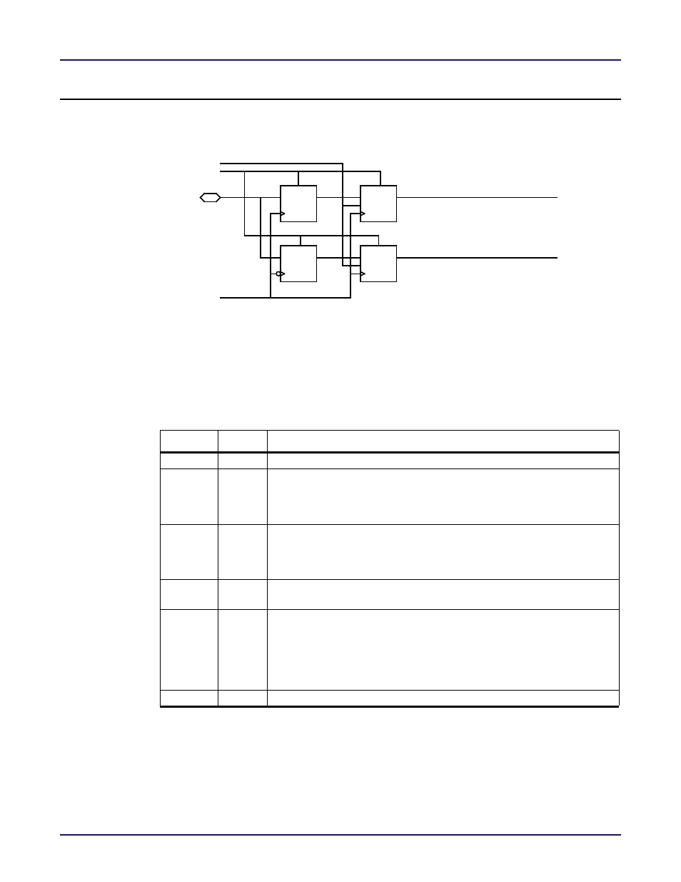
Figure 1-8: IPAD_D2 Logic Symbol
IPAD_D2 is a Double Data Rate (DDR) input pad. There is an additional register stage on the
input to allow the logic level on the pad to changes on both the rising and falling edges of the
clock, but allow the interface signals to and from the FPGA core to change on the rising edge
of the clock. This additional level of registers provides a full cycle to get into and out of the
FPGA core.
Table 1-20: Ports
Name
Type
Description
pad
Bidirectional device pad.
douta
Positive-edge based data output. Data is clocked from the pad to an
internal register on the rising edge of the clock. On the next rising edge of
the clock, if the data_en input is high, the data will appear on the douta
output.
doutb
Negative-edge based data output. Data is clocked from the pad to an
internal register on the falling edge of the clock. On the next rising edge
of the clock, if the data_en input is high, the data will appear on the doutb
output.
data_en
Receive Data Enable (active-high). A high value on rxdata_en enables the
received data to be clocked into the douta and doutb output registers.
rstn
Input Register Reset input. A low value on rstn performs an asynchro-
nous initialization of the Input Register if the rstmode parameter is set to
“async”. A low value on rstn performs a synchronous initialization of the
input registers if the rstmode parameter is set to "sync". The value initial-
ized into the Input Register is determined by the value of the rstvalue
parameter.
clk
Input Register Clock Input.
input
output
output
input
input
input