Heading1 - dffec, Figure - figure 2-3: logic symbol, Heading2 - pins – Achronix Speedster22i User Macro Guide User Manual
Page 69: Table - table 2-7: pin descriptions, Heading2 - parameters, Table - table 2-8: parameters, Heading3 - init, Dffec, Pins, Parameters
Registers
DFFEC
Speedster22i Macro Cell Library
PAGE 53
DFFEC
Positive Clock Edge D-Type Register with Clock Enable and
Synchronous Clear
cn
ce
d
ck
DFFEC
q
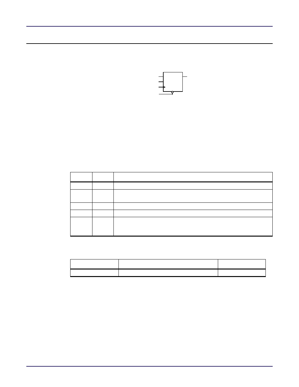
Figure 2-3: Logic Symbol
DFFEC is a single D‐type register with data input (d), clock enable (ce), clock (ck), and active‐
low synchronous clear (cn) inputs and data (q) output. The active‐low synchronous clear
input sets the data output low upon the next rising edge of the clock if it is asserted low and
the clock enable signal is asserted high. If the synchronout clear input is not asserted, the data
output is set to the value on the data input upon the next rising edge of the clock if the active‐
high clock enable input is asserted.
Pins
Table 2-7: Pin Descriptions
Name
Type
Description
d
Data input.
cn
Active-low synchronous clear input. A low on cn sets the q output low
upon the next rising edge of the clock if the clock enable is asserted high.
ce
Active-high clock enable input.
ck
Positive-edge clock input.
q
Data output. The value present on the data input is transferred to the q out-
put upon the rising edge of the clock if the clock enable input is high and the
synchronous clear input is high.
Parameters
Table 2-8: Parameters
Parameter
Defined Values
Default Value
init
1’b0
init
The init parameter defines the initial value of the output of the DFFEC register. This is the
value the register takes upon the initial application of power to the FPGA. The default value
of the init parameter is 1’b0.
input
input
input
input
output
1’b0, 1’b1