Heading3 - timing diagrams, Timing diagrams – Achronix Speedster22i User Macro Guide User Manual
Page 117
Memories
BRAM80K
Speedster22i Macro Cell Library
PAGE 100
correct data at both output ports. In this case, the data corruption will not be noticed by the
circuit until the the corrupted memory location is later read.
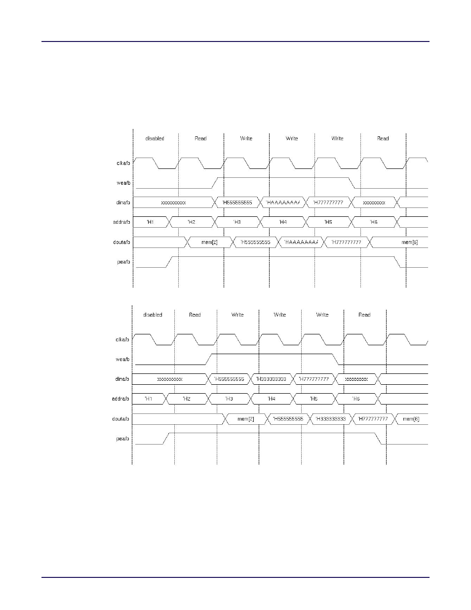
Timing Diagrams
The timing diagrams for the four combinations of the porta_write_mode(portb_write_mode)
and porta_en_out_reg(portb_en_out_reg) parameters is shown below
Figure 6-3: Write-First, Latched Mode Timing Diagram
Figure 6-4: Write-First, Registered Mode Timing Diagram