Heading3 - rdrst_rstval, Heading3 - rdrst_input_mode, Synchronization stage depth – Achronix Speedster22i User Macro Guide User Manual
Page 146
Memories
BRAM80KFIFO
Speedster22i Macro Cell Library
PAGE 129
event when transferring the Write Pointer across clock domains. As an example, setting
wrptr_sync_stages to 2’b00 configures the write pointer synchronization circuit to have two
back‐to‐back registers in the Write Pointer Synchonizer. The default value of the
wrptr_sync_stages parameter is 2’b00.
Table 6-29: Mapping wrptr_sync_stages Parameter Settings to Synchronization Stage Depth
wrptr_sync_stages
Write Pointer Synchronization Stage Depth
2’b00
2
2’b01
3
2’b10
4
2’b11
5
rdrst_rstval
The rdrst_rstval parameter defines the active level of the read port reset (rdrst) input.
Assigning a value of 1’b0 to rdrst_rstval configures the read port reset input to have an active‐
low synchronous reset, while assigning a value of 1’b1 configures the read port reset input to
have an active‐high synchronous reset. The default value of the wrrst_rstval parameter is 1’b1.
rdrst_input_mode
The rdrst_input_mode parameter defines how the Read Pointer is reset. The FIFO macro
provides the user with several options to reset the FIFO either sychronously or to synchronize
the reset input to the appropriate clock domain within the FIFO without the need to
implement separate synchronization circuitry in the FPGA fabric.
The Read Pointer Reset input of the Read Pointer must be synchronous to the rdclk clock
domain. The user must either provide a synchronous reset via the wrrst or rdrst inputs or
synchronize the wrrst input. The method to reset the Read Pointer is selected via the
rdrst_input_mode paramter is defined in
Table 6‐30: rdrst_input_mode Parameter
By configuring the wrrst_input_mode and rdrst_input_mode parameters, the user may
choose to have the FIFO Write Pointer and Read Pointer reset by one or both of the wrrst/rdrst
inputs. Alternatively, the user may also program the reset of the Write Pointer and Read
Pointer independently of each other. For example, the user may program the FIFO reset
inputs to act independently of each other so that the Read Pointer is reset exclusively by the
rdrst input to allow the contents of a previously written FIFO to be reread. Note that as a
result of the Read Pointer reset, the flag outputs are also updated. A block diagram of the
Read Pointer Reset selection circuitry is shown in
Figure 6‐9: Read and Write Pointer Reset
. The default value of the rdrst_input_mode parameter is
2’b10.
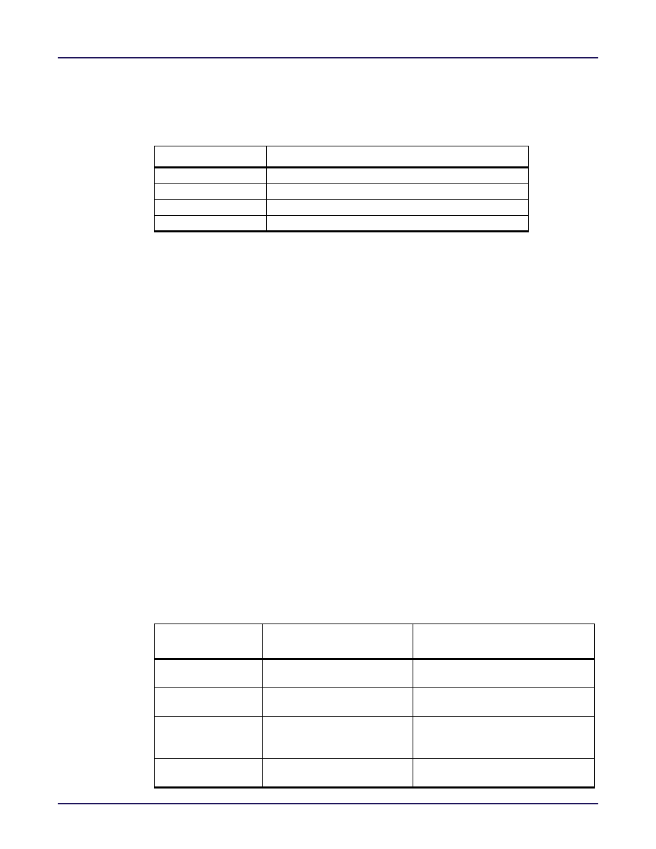
Table 6-30: rdrst_input_mode Parameter Mapping.
rdrst_input_mode
Selected Input for Read
Pointer Reset
Read Pointer Reset Use Model
2’b00
rdrst input resets Read Pointer
Requires rdrst input is synchronous to
rdclk clock domain
2’b01
wrrst input resets Read Pointer
Requires wrrst input is synchronous to
rdclk clock domain
2’b10
rdrst or synchronized wrrst
input resets Read Pointer
Read pointer may be reset by either
the synchronous rdrst or synchonized
wrrst inputs.
2’b11
Synchronized wrrst input resets
Read Pointer
Read Pointer only reset by synchro-
nized wrrst input.