Heading3 - reg_rstval, Heading3 - wrrst_rstval, Heading3 - wrrst_input_mode – Achronix Speedster22i User Macro Guide User Manual
Page 143
Memories
BRAM80KFIFO
Speedster22i Macro Cell Library
PAGE 126
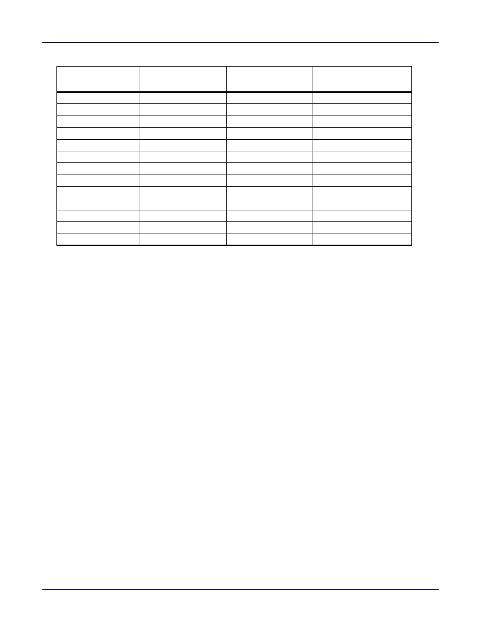
Table 6-25: Relationship of reg_srval bit positions to dout,doutp,doutpx
read_width
doutpx
reg_srval[39:36]
doutp
reg_srval[35:32]
dout
reg_srval[31:0]
40
user_srval[39:36]
user_srval[35:32]
user_srval[31:0]
36
4’hx
user_srval[35:32]
user_srval[31:0]
32
4’hx
4’hx
user_srval[31:0]
20
2’bxx,user_srval[19:18]
2’bxx,user_srval[17:16]
16’hxxxx,user_srval[15:0]
18
4’hx
2’bxx,user_srval[17:16]
16’hxxxx,user_srval[15:0]
16
4’hx
4’hx
16’hxxxx,user_srval[15:0]
10
3’bxxx,user_srval[9]
3’bxxx,user_srval[8]
24’hxxxxxx,user_srval[7:0]
9
4’hx
3’bxxx,user_srval[8]
24’hxxxxxx,user_srval[7:0]
8
4’hx
4’hx
24’hxxxxxx,user_srval[7:0]
5
4’hx
3’bxxx,user_srval[4]
28’hxxxxxxx,user_srval[3:0]
4
4’hx
4’hx
28’hxxxxxxx,user_srval[3:0]
2
4’hx
4’hx
30’hxxxxxxxx,user_srval[1:0]
1
4’hx
4’hx
31’hxxxxxxxx,user_srval[0]
reg_rstval
The reg_rstval parameter defines the active level of the output register rstreg input. Assigning
a value of 1’b0 to reg_rstval configures the output register to have an active‐low synchronous
reset, while assigning a value of 1’b1 configures the output register to have an active‐high
synchronous reset. The default value of the reg_rstval parameter is 1’b1.
regce_priority
The regce_priority parameter defines the priority of the outregce clock enable input relative to
the rstreg reset input during an assertion of the rstreg signal on the output register. Setting
regce_priority to “rstreg” allows the output register to be set/reset at the next active edge of
the rdclk without requiring a specific value on the outregce output register clock enable input.
Setting regce_priority to “regce” requires that the outregce output register clock enable input
is active for the output register set/reset operation to occur at the next active edge of the rdclk.
wrrst_rstval
The wrrst_rstval parameter defines the active level of the write port reset (wrrst) input.
Assigning a value of 1’b0 to wrrst_rstval configures the write port reset input to have an
active‐low synchronous reset, while assigning a value of 1’b1 configures the write port reset
input to have an active‐high reset. The default value of the wrrst_rstval parameter is 1’b1.
wrrst_input_mode
The wrrst_input_mode parameter defines how the Write Pointer is reset. The FIFO macro
provides the user with several options to reset the FIFO either sychronously or to synchronize
the reset input to the appropriate clock domain within the FIFO without the need to
implement separate synchronization circuitry in the FPGA fabric.
The Write Pointer Reset input of the Write Pointer must be synchronous to the wrclk clock
domain. The user must either provide a synchronous reset via the wrrst or rdrst inputs or
synchronize the rdrst input. The method to reset the Write Pointer is selected via the
wrrst_input_mode paramter as defined in
Table 6‐26: wrrst_input_mode Parameter
By configuring the wrrst_input_mode and rdrst_input_mode parameters, the user may
choose to have the FIFO Write Pointer and Read Pointer reset by one or both of the wrrst/rdrst