Rockwell Automation 20D PowerFlex 700S AC Drives with Phase II Control Programming Manual User Manual
Page 68
68
Rockwell Automation Publication 20D-PM001C-EN-P - July 2013
Chapter 2
Programming and Parameters
332
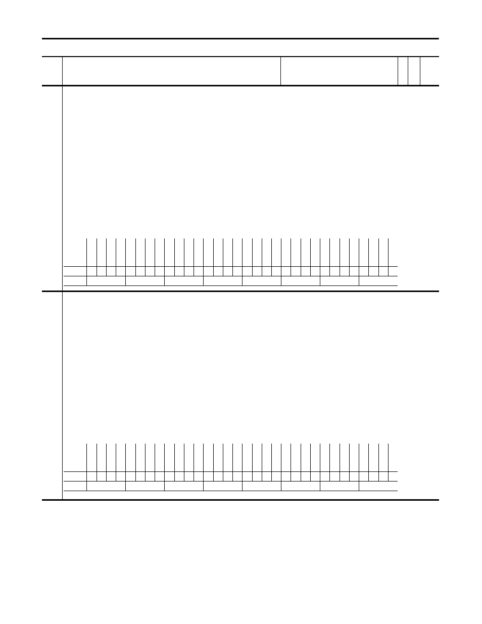
700L EventStatus
Indicates the presence of certain drive anomalies for PowerFlex 700L (LiquiFlo) drive.
• Bit 0 “Dsat Phs U1” indicates that the primary structure detected a Dsat on phase U.
• Bit 1 “Dsat Phs V1” indicates that the primary structure detected a Dsat on phase V.
• Bit 2 “Dsat Phs W” indicates that the primary structure detected a Dsat on phase W.
• Bit 3 “Ovr Current1” indicates that the primary structure detected an over current.
• Bit 4 “Ovr Volt1” indicates that the primary structure detected an over voltage.
• Bit 5 “Asym DcLink1” indicates that the primary structure detected an unbalanced DC Link.
• Bit 6 “Pwr Suply1” indicates that the primary structure detected a power supply failure.
• Bit 7 “HW Disable1” indicates that the primary structure detected a hardware disable.
• Bit 8 “Latch Err1” indicates that the primary structure fault was generated but no indicating bit was set.
• Bit 14 “Cnv NotLogin” the converter was expected but none logged in.
• Bit 15 “Cnv NotStart” the converter was commanded to start but did not become active.
• Bit 16 “Dsat Phs U2” the second structure detected a Dsat on phase U.
• Bit 17 “Dsat Phs V2” the second structure detected a Dsat on phase V.
• Bit 18 “Dsat Phs W2” the second structure detected a Dsat on phase W.
• Bit 19 “Ovr Current2” the second structure detected an over current.
• Bit 20 “Ovr Volt2” the second structure detected an over voltage.
• Bit 21 “Asym DcLink2” the second structure detected an unbalanced DC Link.
• Bit 22 “Pwr Suply2” the second structure detected a power supply failure.
• Bit 23 “HW Disable2” the second structure detected a hardware disable.
• Bit 24 “Latch Err2” the second structure fault was generated but no indicating bit was set.
Note: This parameter was added for firmware version 2.003.
333
700L FaultStatus
Indicates the occurrence of exception events that have been configured as fault conditions for PowerFlex 700L (LiquiFlo) drive.
• Bit 0 “Dsat Phs U1” indicates that the primary structure detected a Dsat on phase U.
• Bit 1 “Dsat Phs V1” indicates that the primary structure detected a Dsat on phase V.
• Bit 2 “Dsat Phs W” indicates that the primary structure detected a Dsat on phase W.
• Bit 3 “Ovr Current1” indicates that the primary structure detected an over current.
• Bit 4 “Ovr Volt1” indicates that the primary structure detected an over voltage.
• Bit 5 “Asym DcLink1” indicates that the primary structure detected an unbalanced DC Link.
• Bit 6 “Pwr Suply1” indicates that the primary structure detected a power supply failure.
• Bit 7 “HW Disable1” indicates that the primary structure detected a hardware disable.
• Bit 8 “Latch Err1” indicates that the primary structure fault was generated but no indicating bit was set.
• Bit 14 “Cnv NotLogin” indicates that the converter expected but none logged in.
• Bit 15 “Cnv NotStart” indicates that the converter commanded to start but did not become active.
• Bit 16 “Dsat Phs U2” indicates that the second structure detected a Dsat on phase U.
• Bit 17 “Dsat Phs V2” indicates that the second structure detected a Dsat on phase V.
• Bit 18 “Dsat Phs W2” indicates that the second structure detected a Dsat on phase W.
• Bit 19 “Ovr Current2” indicates that the second structure detected an over current.
• Bit 20 “Ovr Volt2” indicates that the second structure detected an over voltage.
• Bit 21 “Asym DcLink2” indicates that the second structure detected an unbalanced DC Link.
• Bit 22 “Pwr Suply2” indicates that the second structure detected a power supply failure.
• Bit 23 “HW Disable2” indicates that the second structure detected a hardware disable.
• Bit 24 “Latch Err2” indicates that the second structure fault was generated but no indicating bit was set.
Note: This parameter was added for firmware version 2.003.
No.
Name
Description
Values
Link
able
Re
ad
-Write
Da
ta
T
yp
e
Options
Re
se
rv
ed
Re
se
rv
ed
Re
se
rv
ed
Re
se
rv
ed
Re
se
rv
ed
Re
se
rv
ed
Re
se
rv
ed
Latch
Er
r2
HW Di
sa
bl
e2
Pwr
S
upl
y2
Asym DcLink2
Ov
r V
ol
t2
O
vr C
urr
en
t2
Ds
at
Phs
W2
Ds
at
Phs
V2
Ds
at Phs
U2
Cn
v NotS
tar
t
Cnv N
ot
Lo
gin
Re
se
rv
ed
Re
se
rv
ed
Re
se
rv
ed
Re
se
rv
ed
Re
se
rv
ed
Latch
Er
r1
HW Di
sa
bl
e1
Pwr
S
upl
y1
Asym DcLink1
Ov
r V
ol
t1
O
vr C
urr
en
t1
Ds
at
Phs
W1
Ds
at
Phs
V1
Ds
at Phs
U1
Default
x
x
x
x
x
x
x
0
0
0
0
0
0
0
0
0
0
0
x
x
x
x
x
0
0
0
0
0
0
0
0
0
Bit
31 30 29 28 27 26 25 24 23 22 21 20 19 18 17 16 15 14 13 12 11 10 9
8
7
6
5
4
3
2
1
0
0 = False
1 = True
Options
Res
er
ve
d
Res
er
ve
d
Res
er
ve
d
Res
er
ve
d
Res
er
ve
d
Res
er
ve
d
Res
er
ve
d
La
tc
h Err2
HW D
is
abl
e2
Pw
r Su
pl
y2
Asym D
cLink2
Ov
r V
ol
t2
Ov
r C
urr
en
t2
Dsat Phs W2
Dsat Phs V2
Dsat Phs U2
Cn
v N
otStar
t
Cnv No
tL
og
in
Res
er
ve
d
Res
er
ve
d
Res
er
ve
d
Res
er
ve
d
Res
er
ve
d
La
tc
h Err1
HW D
is
abl
e1
Pw
r Su
pl
y1
Asym D
cLink1
Ov
r V
ol
t1
Ov
r C
urr
en
t1
Dsat Phs W1
Dsat Phs V1
Dsat Phs U1
Default
x
x
x
x
x
x
x
0
0
0
0
0
0
0
0
0
0
0
x
x
x
x
x
0
0
0
0
0
0
0
0
0
Bit
31 30 29 28 27 26 25 24 23 22 21 20 19 18 17 16 15 14 13 12 11 10 9
8
7
6
5
4
3
2
1
0
0 = False
1 = True