Rockwell Automation 20D PowerFlex 700S AC Drives with Phase II Control Programming Manual User Manual
Page 67
Rockwell Automation Publication 20D-PM001C-EN-P - July 2013
67
Programming and Parameters
Chapter 2
No.
Name
Description
Values
Li
nk
ab
le
Re
ad
-W
ri
te
Da
ta
T
ype
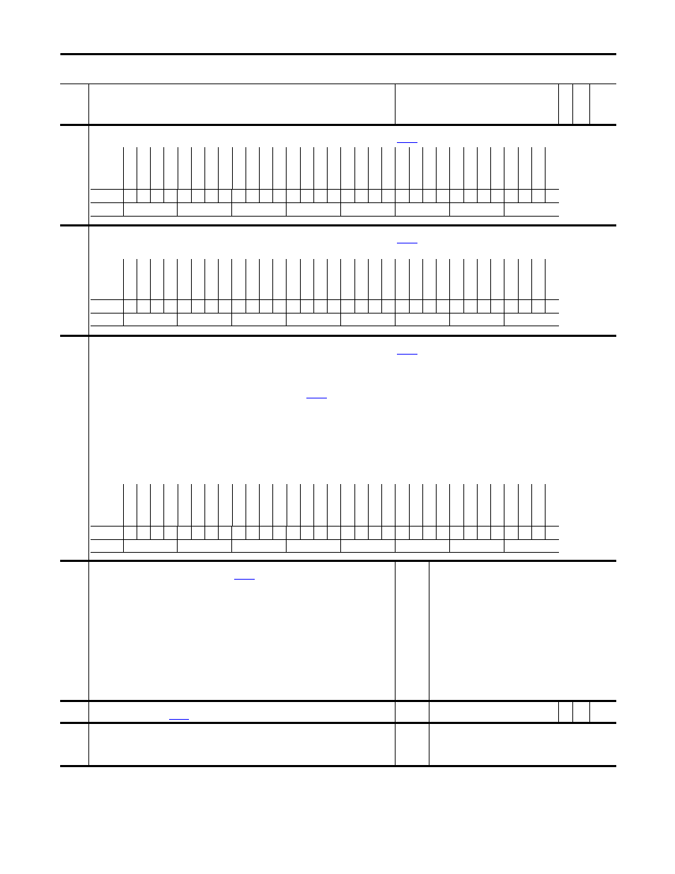
326
Alarm Status 1
Indicates the occurrence of exception events that have been configured as alarm conditions. These events are from
[Exception Event1].
327
Alarm Status 2
Indicates the occurrence of exception events that have been configured as alarm conditions. These events are from
[Exception Event2]
Note: Changed bit 14 to “NonCnfgAlarm” for firmware version 3.003.
328
Alarm Status 3
Indicates the occurrence of exception events that have been configured as alarm conditions. These events are from
[Exception Event3].
• Bit 11 “HH HW Ver” indicates a non-configurable High Horsepower hardware version fault.
• Bit 12 “HH CurUnblnc” indicates a non-configurable High Horsepower output current unbalanced fault.
• Bit 13 “HH VltUnblnc” indicates a non-configurable High Horsepower Bus voltage unbalanced fault.
• Bit 14 “HH Bus Data” indicates when Communication Bus data are mismatched between left side unit and right side unit.
• Bit 21 “Drive Homing” when the drive is in “Drive Homing” mode (parameter
[Position Control] bit 24 “Find Home” or bit 27 “Return Home” is set to “1”) this alarm is triggered and the
drive moves to a home position automatically.
• Bit 24 “Drv Waking” when set, the drive is in wake mode and could start at any time.
• Bit 28 “+/- 12v Pwr” identifies when the12V dc control voltage is outside the tolerance range. The positive voltage power exceeds +15.50 V dc and the negative voltage power exceeds -15.50V
DC.
• Bit 29 “AnlgIn1 Loss” indicates a non-configurable Analog Input 1 loss fault.
• Bit 30 “AnlgIn2 Loss” indicates a non-configurable Analog Input 2 loss fault.
• Bit 31 “AnlgIn3 Loss” indicates a non-configurable Analog Input 3 loss fault.
Notes: Bits 16, 20 and 23 were added for firmware version 2.004. Bits 11, 12, 13, 29, 30 and 31 were added for firmware version 3.001. Changed bit 21 to “Drive Homing” and bit 28 to “+/- 12v Pwr”
for firmware version 3.003. Bit 14 “HH Bus Data” was added for firmware version 3.004. Bit 24 “Drv Waking” and 27 “RideThruAlrm” were added for firmware version 5.002.
329
Fault TP Sel
Enter or write a value to select Fault data displayed in
[Fault TP Data].
• 24 “ElpsSec.mSec” = Elapsed time in seconds and milliseconds since the last power up
• 25 “ElpsMin.Sec” = Elapsed time in minutes and seconds since the last power up
• 26 “ElpsHour.Min” = Elapsed time in hours and minutes since the last power up
• 27 “ElpsDay.Hour” = Elapsed time in days and hours since the last power up
Note: 'Values 24 - 27 were added for firmware version 4.002.
Default:
Options:
0 =
0 =
1 =
2 =
3 =
4 =
5 =
6 =
7 =
8 =
9 =
10 =
11 =
12 =
13 =
“Zero”
“Zero”
14 = “MtrStallTime”
“Abs OverSpd”
15 = “MC Handshake”
“EE Pwr State”
16 = “VPL Handshak”
“Inv DataStat”
17 = “MC Diag”
“Run Time Err”
18 = “PwrLossState”
“LowBus Thres”
19 = “12 volt loss”
“LowBus Detct”
20 = “PwrEE Chksum”
“PwrLosBusVlt”
21 = “Db Read Cnt1”
“MCPLosBusVlt”
22 = “Db Read Cnt2”
“MC Flt Reset”
23 = “Db Read Cnt3”
“Ext Flt Stat”
24 = “ElpsSec.mSec”
“VPL TaskErr”
25 = “Elps Min.Sec”
“Mtr OL Input”
26 = “ElpsHour.Min”
“Mtr OL Outpt”
27 = “ElpsDay.Hour”
330
Fault TP Data
Displays the data selected by
[Fault TP Sel].
Default:
Min/Max:
0
-/+2200000000
RO
Real
331 LstFaultStopMode
Displays the action taken by the drive during the last fault. When a fault occurs, an action is taken as a result of
that fault.
Default:
Options:
0 =
0 =
1 =
2 =
“Ignore”
“Ignore”
3 = “Flt RampStop“
“Alarm”
4 = “FltCurLimStop”
“FltCoastStop”
Options
NonC
nfg F
ault
Pr
echar
ge
E
r
NonC
nfg F
ault
NonC
nfg F
ault
NonC
nfg F
ault
NonC
nfg F
ault
NonC
nfg F
ault
NonC
nfg F
ault
NonC
nfg F
ault
NonC
nfg F
ault
NonC
nfg F
ault
Ine
rtia
T
es
t
NonC
nfg F
ault
NonC
nfg F
ault
Ex
t F
ault In
In
v O
L T
rip
In
v O
L P
end
Non C
nfg F
ault
In
v T
empP
end
Mot
or Sta
ll
Mtr OL
P
en
d
Mtr OL
T
rip
NonC
nfgF
ault
SLink C
omm
NonC
nfgF
ault
NonC
nfgF
ault
FB Opt 1 L
oss
FB Opt0 L
oss
Enc
dr1 L
oss
Enc
dr0 L
oss
NonC
nfgF
ault
NonC
nfgF
ault
Default
0
0
0
0
0
0
0
0
0
0
0
0
0
0
0
0
0
0
0
0
0
0
0
0
0
0
0
0
0
0
0
0
Bit
31 30 29 28 27 26 25 24 23 22 21 20 19 18 17 16 15 14 13 12 11 10 9
8
7
6
5
4
3
2
1
0
0 = False
1 = True
Options
Lg
x LinkChng
Lg
x C
lo
se
d
Lg
x T
imeout
Lg
x O
ut
O
fR
un
Net
Lo
ss DP
I6
Net
Lo
ss DP
I5
Net
Lo
ss DP
I4
Net
Lo
ss DP
I3
Net
Lo
ss DP
I2
Net
Lo
ss DP
I1
DPI
L
os
s P6
DPI
L
os
s P5
DPI
L
os
s P4
DPI
L
os
s P3
DPI
L
os
s P2
DPI
L
os
s P1
N
onC
nfg F
ault
MC
C
M
L F
ail
Inte
rp S
ynch
En
abl
eH
eal
th
Runti
m
e Da
ta
Vo
ltF
dbkL
oss
Bus
U
nderV
olt
N
onC
nfg F
ault
Slink Mult
N
onC
nfg F
ault
Brak
eO
L T
rip
N
onC
nfg F
ault
N
onC
nfg F
ault
N
onC
nfg F
ault
M
C C
omma
nd
N
onC
nfg F
ault
Default
0
0
0
0
0
0
0
0
0
0
0
0
0
0
0
0
0
0
0
0
0
0
0
0
0
0
0
0
0
0
0
0
Bit
31 30 29 28 27 26 25 24 23 22 21 20 19 18 17 16 15 14 13 12 11 10 9
8
7
6
5
4
3
2
1
0
0 = False
1 = True
Options
No
nC
nfg
F
au
lt
No
nC
nfg
F
au
lt
No
nC
nfg
F
au
lt
+/
- 12v
P
w
r
Ri
de
Th
ruA
lrm
Re
se
rv
ed
Re
se
rv
ed
Dr
v W
ak
in
g
St
ah
l O
pt
ic
s
Re
se
rv
ed
Dr
iv
e Ho
m
in
g
Po
si
t E
rr
-Hr
d O
vr
Tr
vl
+H
rd O
vr
Tr
vl
-Sf
t O
vr
Tr
vl
+Sf
t O
vr
Tr
vl
Re
se
rv
ed
HH
Bus Da
ta
HH
V
ltUnbl
nc
HH C
urrUnblnc
HH
HW V
er
No
nC
nfg
F
au
lt
No
nC
nfg
F
au
lt
No
nC
nfg
F
au
lt
No
nC
nfg
F
au
lt
No
nC
nfg
F
au
lt
No
nC
nfg
F
au
lt
No
nC
nfg
F
au
lt
No
nC
nfg
F
au
lt
No
nC
nfg
F
au
lt
No
nC
nfg
F
au
lt
HH
InPha
se
Ls
Default
0
0
0
0
0
x
x
0
0
0
0
0
0
0
0
0
x
0
0
0
0
0
0
0
0
0
0
0
0
0
0
0
Bit
31 30 29 28 27 26 25 24 23 22 21 20 19 18 17 16 15 14 13 12 11 10 9
8
7
6
5
4
3
2
1
0
0 = False
1 = True