Block diagrams – Rockwell Automation 20G PowerFlex 750-Series AC Drives User Manual
Page 150
150
Rockwell Automation Publication 750-RM002B-EN-P - September 2013
Chapter 2
Feedback and I/O
Block Diagrams
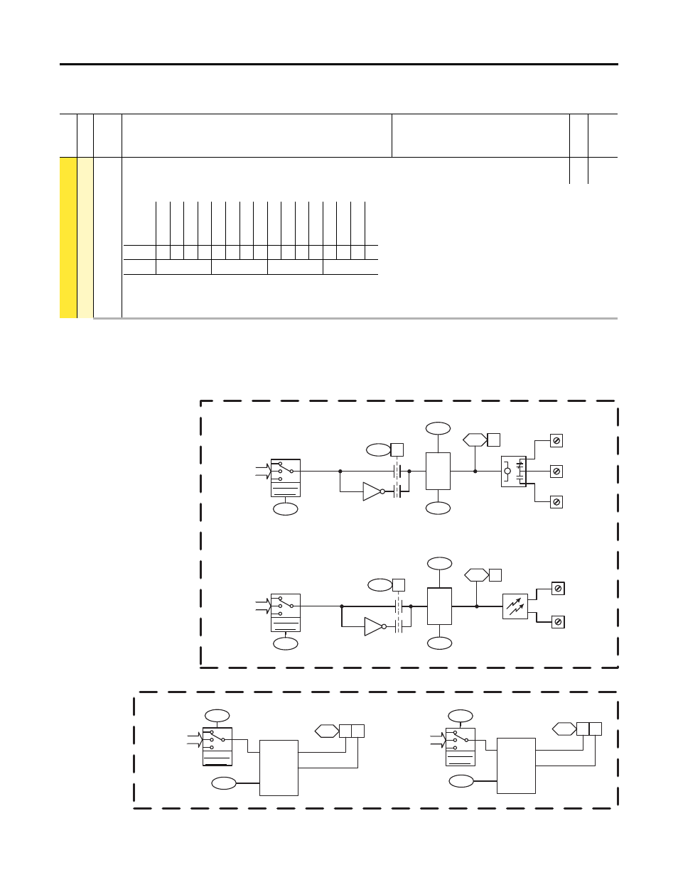
Figure 11 - PowerFlex 753 Drive
Fil
e
Gr
ou
p
No.
Display Name
Full Name
Description
Values
Re
ad
-Write
Da
ta T
ype
I/O
D
igi
ta
l O
u
tpu
ts
5
Dig Out Sts
Digital Output Status
RO
16-bit
Integer
Status of the digital outputs.
(1) Bit 1 = “Trans Out 0” for I/O Module model 20-750-2263C-1R2T.
= “Relay Out 1” for I/O Module models 20-750-2262C-2R and 20-750-2262D-2R.
(2) Bit 2 is used only by I/O Module 20-750-2263C-1R2T.
Options
Re
ser
ved
Re
ser
ved
Re
ser
ved
Re
ser
ved
Re
ser
ved
Re
ser
ved
Re
ser
ved
Re
ser
ved
Re
ser
ved
Re
ser
ved
Re
ser
ved
Re
ser
ved
Re
ser
ved
Tr
an
s O
ut
1
(2
)
Tr
an
s O
ut
0
(1
)
Re
la
y O
ut
0
Default
0
0
0
0
0
0
0
0
0
0
0
0
0
0
0
0
Bit
15 14 13 12 11 10 9
8
7
6
5
4
3
2
1
0
0 = Output De-energized
1 = Output Energized
225
0
234
235
232
A
B
230
226
0
0
1
233
1
A 0 231 242 A B 243 1 0 225 1 224 245 226 1 0 1 240 241 A≥B A A≥B RO0 Off Time Timer Dig Out Sts Dig Out Invert RO0 On Time Inv Parameter Selection Parameter Selection Parameter Selection Parameter Selection Inv TO0 Off Time Timer Dig Out Sts Dig Out Invert TO0 On Time Relay Out0 Source Transistor Out0 Source RO0 Level Source RO0 Sel TO0 Sel RO0 Level Sel RO0 Level CmpSts RO0 Level TO0 Level Source TO0 Level Sel TO0 Level CmpSts TO0 Level NC Common NO 24V Common NO