Spibus decode setup detail, Operator's manual – Teledyne LeCroy Serial Data Debug Solutions User Manual
Page 59
Operator's Manual
919586 RevA
59
The SPI trigger does not require use of a Chip Select line. In its place is the ability to set a minimum Interframe
Time corresponding with a time that (in AUTO mode) is (typically) 4x a single bit time and less than the
interframe time between different message packets. By eliminating the Chip Select line presence requirement,
an additional oscilloscope channel is preserved for use with other analog signals. This is a significant feature. It
also allows a user to trigger on simplified SPI (SSPI, SIOP, etc.) protocols with a single Master and Slave and no
Chip Select line.
Note: Ask your local LeCroy representative for more information about any Serial Data Debug Solution
Protocols or Toolkits using the Contact LeCroy for Support (on page 199) topic.
SPIbus Decode Setup Detail
For general information about using controls shown on the main Serial Decode dialog, refer to Accessing The D
and TD Supported Protocol Toolsets (on page 13).
SPI
BUS
SPI
AND
L
EVELS
R
IGHT
-H
AND
D
IALOGS
Access the Serial Decode dialog by touching Analysis → Serial Decode on the menu bar.
Touch the corresponding Setup... button for your decode. The Decode Setup... along with corresponding right-
hand dialogs are shown.
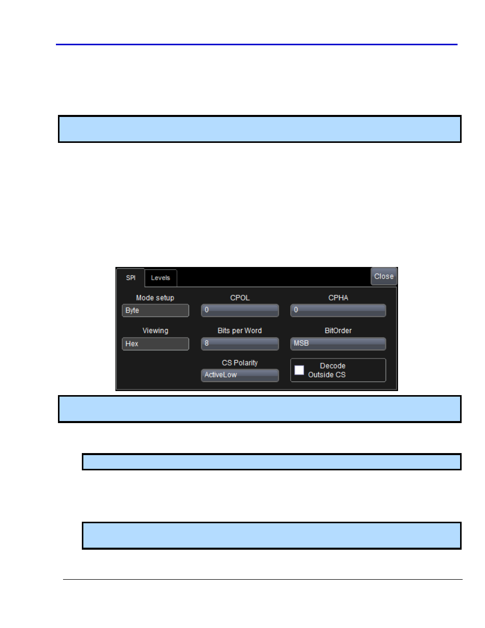
SPIbus SPI Right-Hand Dialog
The SPI right-hand dialog provides detailed controls and setup conditions as follows:
Note: A similar dialog is shown when SSPI or SIOP are selected; however, these protocols do not use a Chip
Select, so the Chip Select selections are omitted.
Mode setup - Configure your decode setup relative to Byte or Frame using this control.
Viewing - Select to view the protocol data in Binary, Hexadecimal, ASCII, or Decimal modes.
Note: If the trigger is set up first, the trigger settings copy into the decode settings.
Clock Polarity and Phase - SPI requires that selections be made for the clock polarity and phasing of the
data to the clock. SPI microcontrollers and peripherals have settings for CPOL (Clock Polarity) and CPHA
(Clock Phase) that are published in the technical datasheets for those products. These values need to be
entered in this section.
Note: SPI Mode 0 = CPOL 0 and CPHA 0. SPI Mode 1 = CPOL 0 and CPHA 1. SPI Mode 2 = CPOL 1 and
CPHA 0. SPI Mode 3 = CPOL 1 and CPHA 1.