Cache line size, Latency timer, Register: 0x0c – Avago Technologies LSI53C1020 User Manual
Page 86: Register: 0x0d
4-8
PCI Host Register Description
Version 2.4
Copyright © 2001–2004 by LSI Logic Corporation. All rights reserved.
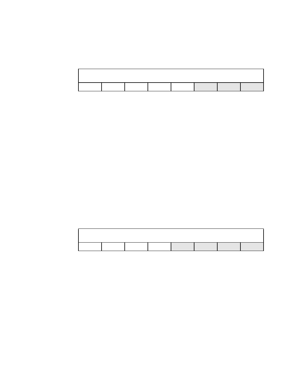
Register: 0x0C
Cache Line Size
Read/Write
Cache Line Size
[7:3]
This 8-bit register specifies the system cache line size in
units of 32-bit words. In the conventional PCI mode, the
LSI53C1020 PCI function uses this register to determine
whether to use Write and Invalidate or Write commands
for performing write cycles. Programming this register to
a number other than a nonzero power of two disables the
the use of the PCI performance commands to execute
data transfers. The PCI function ignores this register
when operating in the PCI-X mode.
Reserved
[2:0]
This field is reserved.
Register: 0x0D
Latency Timer
Read/Write
Latency Timer
[7:4]
This 8-bit register specifies, in units of PCI bus clocks, the
value of the Latency Timer for this PCI bus master. If the
LSI53C1020 initializes in the PCI mode, the default value
of this register is 0x00. If the LSI53C1020 initializes in the
PCI-X mode, the default value of this register is 0x40.
Reserved
[3:0]
This field is reserved.
7
3
2
0
Cache Line Size
0
0
0
0
0
0
0
0
7
4
3
0
Latency Timer
0
X
0
0
0
0
0
0