Avago Technologies LSI53C1020 User Manual
Page 125
DC Characteristics
5-5
Version 2.4
Copyright © 2001–2004 by LSI Logic Corporation. All rights reserved.
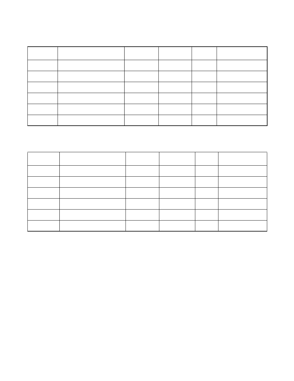
Table 5.7
8 mA Bidirectional Signals – GPIO[7:0], MAD[15:0], MADP[1:0], SerialDATA
Symbol
Parameter
Min
Max
Unit
Test Conditions
V
IH
Input high voltage
2.0
3.6
V
–
V
IL
Input low voltage
−
0.3
0.8
V
–
V
OH
Output high voltage
2.4
VDD
V
−
8 mA
V
OL
Output low voltage
VSS
0.4
V
8 mA
I
OZ
3-state leakage
−
10
10
µ
A
V
PIN
= 0 V, 5.25 V
I
PULL
Pull-up current
25
–
µ
A
–
Table 5.8
8 mA PCI Bidirectional Signals – ACK64/, AD[63:0], C_BE[7:0]/, DEVSEL/,
FRAME/, IRDY/, PAR, PAR64, PERR/, REQ64/, SERR/, STOP/, TRDY/
Symbol
Parameter
Min
Max
Unit
Test Conditions
V
IH
Input high voltage
0.5 VDD
PCI5VBIAS
1
1. The maximum PCI input voltage depends upon the operating mode of the PCI bus, which
PCI5VBIAS determines. The maximum input voltage in a 5 V PCI system is 5 V. The maximum input
voltage in a 3.3 V PCI system is VDD. Refer to the signal description in
Section 3.9, “Power and Ground Pins,” page 3-16
, for more information concerning PCI5VBIAS.
V
–
V
IL
Input low voltage
−
0.5
0.3 VDD
V
–
V
OH
Output high voltage
0.9 VDD
VDD
V
−
500
µ
A
V
OL
Output low voltage
VSS
0.1 VDD
V
1500
µ
A
I
OZ
3-state leakage
−
10
10
µ
A
V
PIN
= 0 V, 5.25 V
I
PULL-DOWN
Pull-down current
2
2. Pull-down text does not apply to AD[31:0] and C_BE[3:0]/.
25
–
µ
A
–