Figure5.2 lvd receiver, Table5.5 diffsens scsi signal, Table5.6 input capacitance – Avago Technologies LSI53C1020 User Manual
Page 124: Lvd receiver, Lvd receiver scsi signals – sack, Diffsens scsi signal, Input capacitance
5-4
Specifications
Version 2.4
Copyright © 2001–2004 by LSI Logic Corporation. All rights reserved.
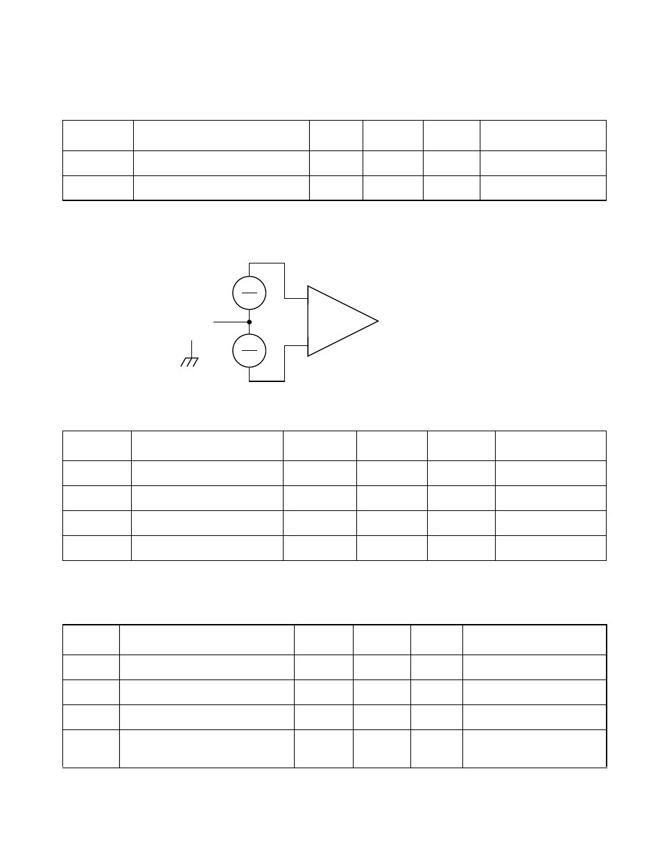
Figure 5.2
LVD Receiver
Table 5.4
LVD Receiver SCSI Signals
1
– SACK
±
, SATN
±
, SBSY
±
, SCD
±
, SD[15:0]
±
,
SDP[1:0]
±
, SIO
±
, SMSG
±
, SREQ
±
, SRST
±
, SSEL
±
1. V
CM
= 0.7–1.8 V (Common Mode Voltage, nominal ~1.2 V.)
Symbol
Parameter
Min
Max
Unit
Test Conditions
V
I
LVD receiver voltage asserting
|30|
–
mV
Differential voltage
V
I
LVD receiver voltage negating
−
|
30|
mV
Differential voltage
V
CM
+
−
+
+
+
−
−
−
V
I
2
V
I
2
Table 5.5
DIFFSENS SCSI Signal
Symbol
Parameter
Min
Max
Unit
Test Conditions
V
IH
HVD sense voltage
2.4
3.6
V
See note
1
1. V
IH
, V
IL
, and V
s
are specified in the SPI-4 draft specification.
V
S
LVD sense voltage
0.7
1.9
V
See note
1
V
IL
SE sense voltage
VSS
−
0.35
0.5
V
See note
1
I
OZ
3-state leakage
−
10
10
µ
A
V
PIN
= 0 V, 3.6 V
Table 5.6
Input Capacitance
Symbol
Parameter
Min
Max
Unit
Test Conditions
C
I
Input capacitance of input pads
–
7
pF
Guaranteed by design
C
IO
Input capacitance of I/O pads
–
15
pF
Guaranteed by design
C
PCI
Input capacitance of PCI pads
–
8
pF
Guaranteed by design
C
LVD
Input capacitance of LVD pads
–
8
pF
6.5 pF pad;
1.5 pF package