4 scsi interface signals, Table3.8 scsi bus clock signal, Table3.9 scsi channel interface signals – Avago Technologies LSI53C1020 User Manual
Page 65: Scsi interface signals, Scsi bus clock signal, Scsi channel interface signals, Section 3.4, “scsi interface signals
SCSI Interface Signals
3-9
Version 2.4
Copyright © 2001–2004 by LSI Logic Corporation. All rights reserved.
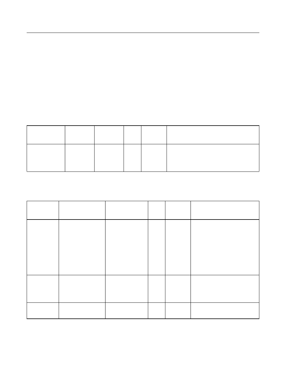
3.4
SCSI Interface Signals
This section describes the signals for the SCSI Channel interface.
describes the SCSI bus interface clock signal.
In LVD mode, the negative and positive signals form the differential pair.
In SE mode, the negative signals represent the signal pin and the
positive signals are a virtual ground. The LSI53C1020 does not support
HVD mode. If HVD signaling is present, the SCSI channel 3-states its
drivers.
describes the SCSI Channel Interface signals group.
Table 3.8
SCSI Bus Clock Signal
Signal Name
456-Ball
Package
384-Ball
Package
Type
Strength Description
SCLK
F3
B4
I
N/A
SCSI Clock provides the 80 MHz
reference clock source for the
ARM966E-S processors and all SCSI-
related timings.
Table 3.9
SCSI Channel Interface Signals
Signal
Name
456-Ball
Package
384-Ball
Package
Type
Strength Description
SD[15:0]
−
SD[15:0]+
Y1, AA2, AB2,
AD1, F2, G2, J4,
H1, R4, T5, T2,
U2, U5, V2, V4,
W4
W5, Y2, AA3, AC1,
D1, G1, H4, H2,
P3, R5, R2, T4,
U4, U3, V5, V3
Y1, Y4, AA1,
AA4, F2, G4, G2,
H4, R2, R3, T2,
T3, U2, V1, V4,
W1
W3, Y2, Y3, AA2,
F3, F1, G3, G1,
R1, R4, T1, T4,
U1, U3, V2, V3
I/O
SE:
48 mA
LVD:
12 mA
SCSI Channel Data signals.
SDP[1:0]
−
SDP[1:0]+
W2, P4
W1, P5
W4, P3
W2, P2
I/O
SE:
48 mA
LVD:
12 mA
SCSI Channel Data Parity
signals.
VDDBIAS
T1
N2
P
N/A
Provides power for the
RBIAS circuit.