7 test interface, Table3.14 jtag, ice, and debug signals, Test interface – Avago Technologies LSI53C1020 User Manual
Page 70: Jtag, ice, and debug signals, Section 3.7, “test interface
3-14
Signal Description
Version 2.4
Copyright © 2001–2004 by LSI Logic Corporation. All rights reserved.
3.7
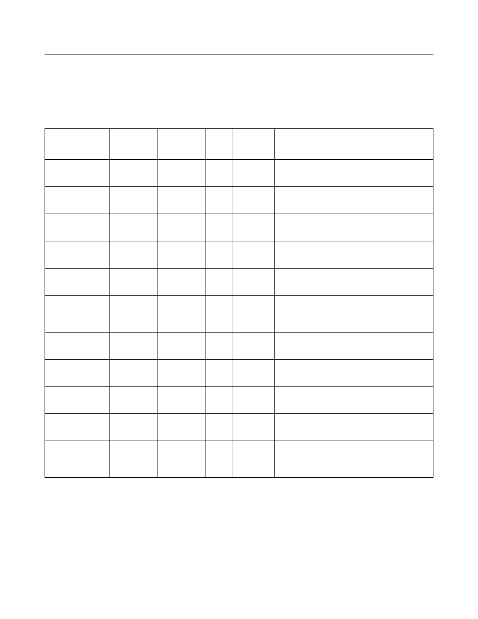
Test Interface
describes the JTAG, ICE, and Debug signals group.
Table 3.14
JTAG, ICE, and Debug Signals
Signal Name
456-Ball
Package
384-Ball
Package
Type Strength Description
TST_RST/
AD5
AC8
I
N/A
Active LOW Test Reset is for test
purposes.
TCK_CHIP
AC6
AE8
I
N/A
Chip Test Clock provides a JTAG test
clock signal.
TDI_CHIP
AF3
AD9
I
N/A
Chip Test Data In provides the JTAG
test data in signal.
TDO_CHIP
AD6
AD10
O
8 mA
Chip Test Data Out provides the JTAG
test data out signal.
TMS_CHIP
AE4
AF8
I
N/A
Chip Test Mode Select provides the
JTAG test mode select signal.
RTCK_ICE
AA5
AD6
O
8 mA
Test Clock Acknowledge provides the
JTAG test clock acknowledge signal for
the ICE debug logic.
TRST_ICE/
AB4
AF5
I
N/A
Test Reset provides the JTAG test reset
signal for the ICE debug logic.
TCK_ICE
AA4
AE4
I
N/A
Test Clock provides the JTAG test clock
signal for the ICE debug logic.
TDI_ICE
AB3
AD5
I
N/A
Test Data In provides the JTAG test
data in signal for the ICE debug logic.
TDO_ICE
AD2
AE5
O
8 mA
Test Data Out provides the JTAG test
data out signal for the ICE debug logic.
TMS_ICE
Y5
AF4
I
N/A
Test Mode Select provides the test
mode select signal for the ICE debug
logic.