8 multi-ice test interface, Multi-ice test interface, Section 2.8, “multi-ice test interface – Avago Technologies LSI53C1020 User Manual
Page 55
Multi-ICE Test Interface
2-29
Version 2.4
Copyright © 2001–2004 by LSI Logic Corporation. All rights reserved.
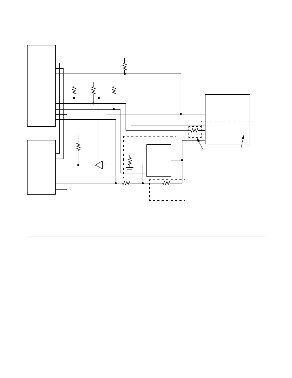
Figure 2.6
ZCR Circuit Diagram for the LSI53C1020 and LSI53C1000R
2.8
Multi-ICE Test Interface
This section describes the LSI Logic requirements for the Multi-ICE test
interface. LSI Logic recommends routing all test signals to a header on
the board.
The Multi-ICE test interface header is a 20-pin header for Multi-ICE
debugging through the ICE JTAG port. This header is essential for
debugging both the firmware and the design functionality and must be
included in board designs. The connector is a 20-pin header that mates
with the IDC sockets mounted on a ribbon cable.
details the
pinout of the 20-pin header.
ZCR PCI
Slot
LSI53C1000R/
Host System
IDSEL
Int A/ (A6)
Int B/ (B7)
Int C/ (A7)
INTA/
Int A/
Int B/
Int C/
TDI (A4)
TMS (A3)
GNT/ (A17)
ZCR_EN/
IOPD_GNT
No Pop for
No Pop for LSI53C1020
2:1 Mux
A0
A1
S0
B0
Vdd
Vdd
LSI53C1020 Only
No Pop for
AD19
AD21
AD21 (B29)
IDSEL (A26)
4.7 k
Ω
Vdd
4.7 k
Ω
Vdd
4.7 k
Ω
Vdd
0.1 k
Ω
0
Ω
0.1 k
Ω
Note:
To maintain proper interrupt mapping, select the address line for use as IDSEL on the
LSI53C1000R/LSI53C1020 to be +2 address lines above IDSEL on ZCR slot.
0.1 k
Ω
0
Ω
LS53C1000R
LSI53C1000R
LSI53C1020
220
Ω
Int D/ (B8)
Int D/