Message address, Message upper address, Register: 0xxx – Avago Technologies LSI53C1020 User Manual
Page 103
PCI Configuration Space Register Descriptions
4-25
Version 2.4
Copyright © 2001–2004 by LSI Logic Corporation. All rights reserved.
Register: 0xXX
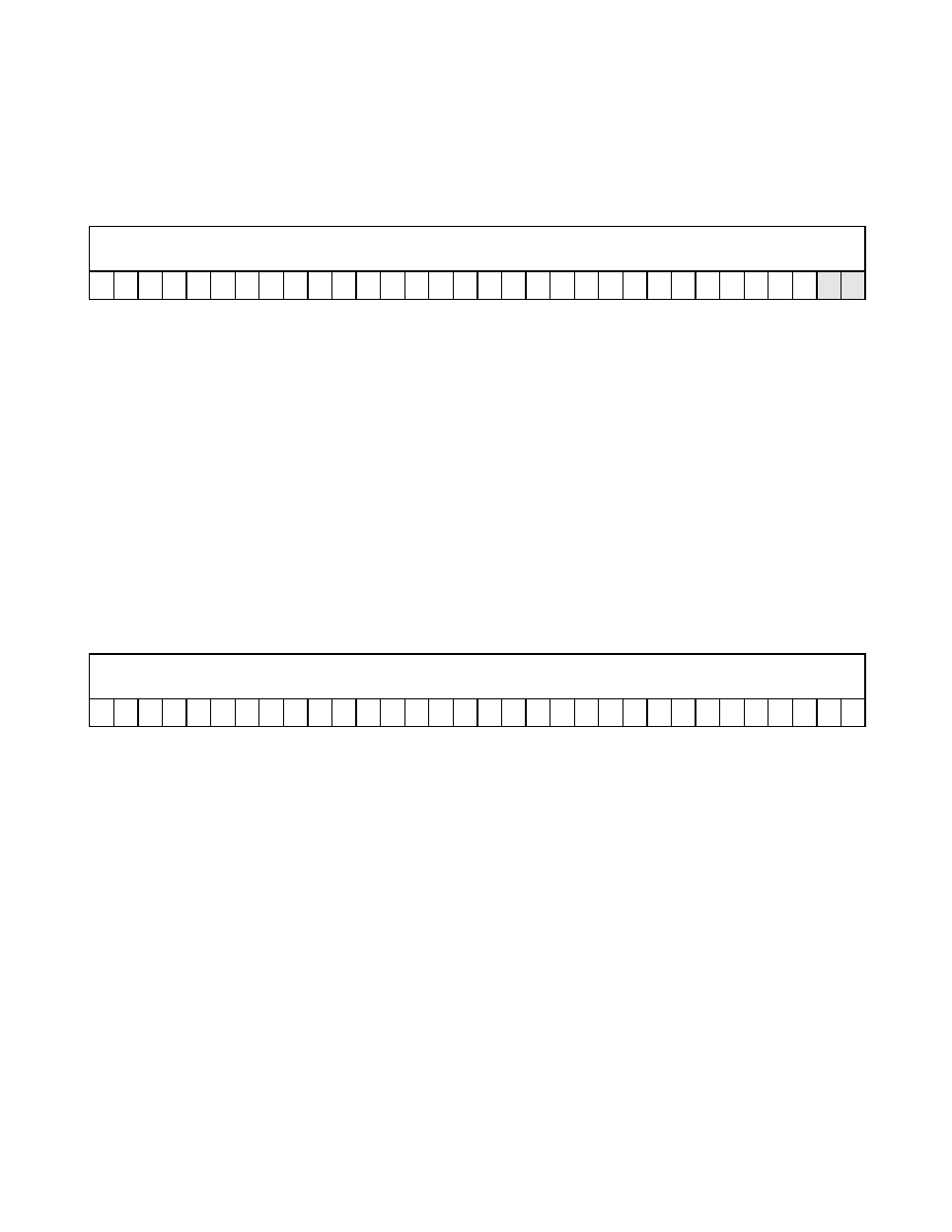
Message Address
Read/Write
Message Address
[31:2]
This field contains message address bits [31:2] for the
MSI memory write transaction. The host system specifies
and dword aligns the message address. During the
address phase, the LSI53C1020 drives Message
Address[1:0] to 0b00.
Reserved
[1:0]
This field is reserved.
Register: 0xXX
Message Upper Address
Read/Write
Message Upper Address
[31:0]
The LSI53C1020 supports 64-bit MSI. This 32-bit register
contains the upper 32 bits of the 64-bit message address,
which the system specifies. The host system software
can program this register to 0x0000 to force the PCI func-
tion to generate 32-bit message addresses.
31
2
1
0
Message Address
0
0
0
0
0
0
0
0
0
0
0
0
0
0
0
0
0
0
0
0
0
0
0
0
0
0
0
0
0
0
0
0
31
0
Message Upper Address
0
0
0
0
0
0
0
0
0
0
0
0
0
0
0
0
0
0
0
0
0
0
0
0
0
0
0
0
0
0
0
0