Viterbi decoder, A.2.2.2 viterbi decoder – Comtech EF Data C5 User Manual
Page 268

Options
C5/K1/K3 Integrated Satellite Terminal System
A–24
Rev. 0
The corrected data is buffered through the output RAM and re-timing circuit, which
provides a data stream to the differential decoder and descrambler at the constant rate of
the data clock. The data and the clock are then output from the card.
The sequential decoder also provides a lock detect signal to the M&C when the error rate
has dropped below a threshold level. The M&C monitors these signals and takes
appropriate action.
The raw BER count is made by comparing the input and output decoder data. Because the
output data contains many fewer errors than the input, differences in the two can be
counted to yield the raw BER. The raw BER is sent to the M&C for further processing.
A.2.2.2 Viterbi
Decoder
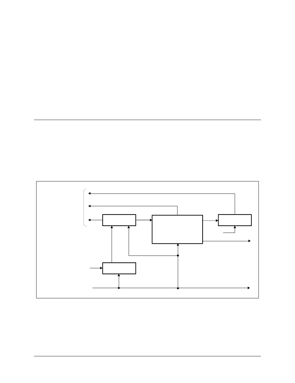
The Viterbi decoder operates in conjunction with the convolutional encoder at the
transmit modem. The decoder uses a decoding algorithm to provide FEC on the received
data stream for errors occurring in the transmission channel.
A block diagram of the Viterbi decoder is shown in Figure A-5.
TO
MICROCOMPUTER
INTERFACE
CONTROL I/O
DEPUNCTURE
PROCESSOR
VITERBI DECODER
WITH
V.35 DESCRAMBLER
AND CHANNEL
BER DETECTION
LOCK DETECT
FROM
COSTAS
PROC.
RX DATA
RX CLOCK
AMBIGUITY
RESOLVER
FROM
INPUT BUFFER
FROM
CLK RECOVERY
Figure A-5. Viterbi Decoder Block Diagram
