NEC PD17062 User Manual
Page 94
94
µ
PD17062
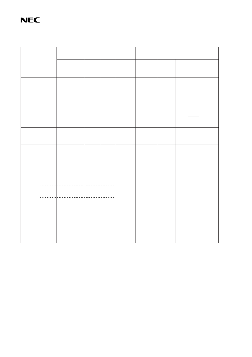
Table 10-1 Peripheral Hardware and Data Buffer Functions
Data buffer and data transfer
Function
peripheral register
Peripheral hardware
Name
Symbol
Peri-
PUT
Data
Valid
Explanation
pheral instruction/
buffer
bits
address
GET
I/O bits
instruction
Image display
IDC start posi- IDCORG
01H
PUT/GET
8
7
Sets the image display
controller
tion setting
controller display start
register
position.
A/D converter
A/D converter
ADCR
02H
PUT/GET
8
4
Sets the AD converter
V
REF
data
comparison voltage
register
V
REF
.
V
REF
=
x – 0.5
×
V
DD
(V)
16
1
≤
x
≤
15
Serial interface
Presettable
SIO0SFR
03H
PUT/GET
8
8
Sets the serial out data
shift register
and reads the serial in
data.
Horizontal syn-
HSYNC
HSC
04H
GET
8
6
Reads the value of the
chronizing signal
counter data
horizontal synchroni-
counter
register
zing signal counter.
PWM
0
PWM data
PWMR0
05H
PUT/GET
8
7
Sets the D/A converter
pin
register 0
output signal duty.
PWM
1
PWM data
PWMR1
06H
Duty D =
x + 0.75
(%)
pin
register 1
64
PWM
2
PWM data
PWMR2
07H
0
≤
x
≤
63
pin
register 2
Frequency f = 15.625 kHz
PWM
3
PWM data
PWMR2
08H
pin
register 3
Address register
Address
AR
40H
PUT/GET
16
16
Reads of writes data
register
from or to the address
register.
PLL frequency
PLL data
PLLR
41H
PUT/GET
16
16
Sets the PLL frequency
synthesizer
register
synthesizer frequency
division ratio.
6-bit
D/A
conver-
ter
(PWM
output)