Standby, 1 standby block configuration – NEC PD17062 User Manual
Page 153

153
µ
PD17062
13. STANDBY
The standby function is intended to reduce the current drain of the device at backup.
13.1 STANDBY BLOCK CONFIGURATION
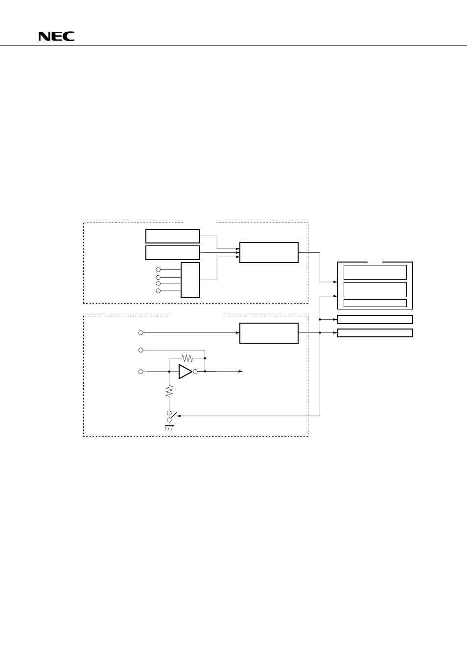
Fig. 13-1 shows the configuration of the standby block.
As shown in Fig. 13-1, the standby block is further divided into halt control and clock stop control blocks.
The halt control block consists of the halt control circuit, interrupt control block, timer carry FF, and the P0D
0
/
ADC
2
to P0D
3
/ADC
5
pins. It controls the operation of the CPU (program counter, instruction decoder, and ALU
block).
The clock stop control block controls the 8 MHz crystal oscillator, CPU, system register, and control register.
Fig. 13-1 Standby Block Configuration
ALU
Halt block
Interrupt block
Timer carry FF
Halt control circuit
HALT h
P0D
3
/ADC
5
pin
P0D
2
/ADC
4
pin
P0D
1
/ADC
3
pin
P0D
0
/ADC
2
pin
Input latch
Program counter (PC)
Instruction decoder
Clock stop block
System register
CE pin
Clock stop
control circuit
STOP s
Control register
X
OUT
pin
X
IN
pin
Internal clock
CPU
