5 character rom – NEC PD17062 User Manual
Page 255
255
µ
PD17062
20.5 CHARACTER ROM
The CROM (character ROM) consists of the IDC pattern data and control data. The CROM data shares the
program memory with programs. The CROM area has a capacity of 2 Ksteps (1920
×
16 bits). An area not
used as CROM is used as an ordinary program area.
The CROM area in ROM is at 0800H to 0F7FH. The CROM area is divided into BANK0 and BANK1. A concept
of bank applies only to CROM. It does not apply to a program area. CROM BANK0 is 1 Kword at from 0800H
to 0BFFH, and CROM BANK1 is 896 words at from 0C00H to 0F7FH.
The CROM bank is switched according to the CROMBNK flag (b
0
at 30H) in the register file.
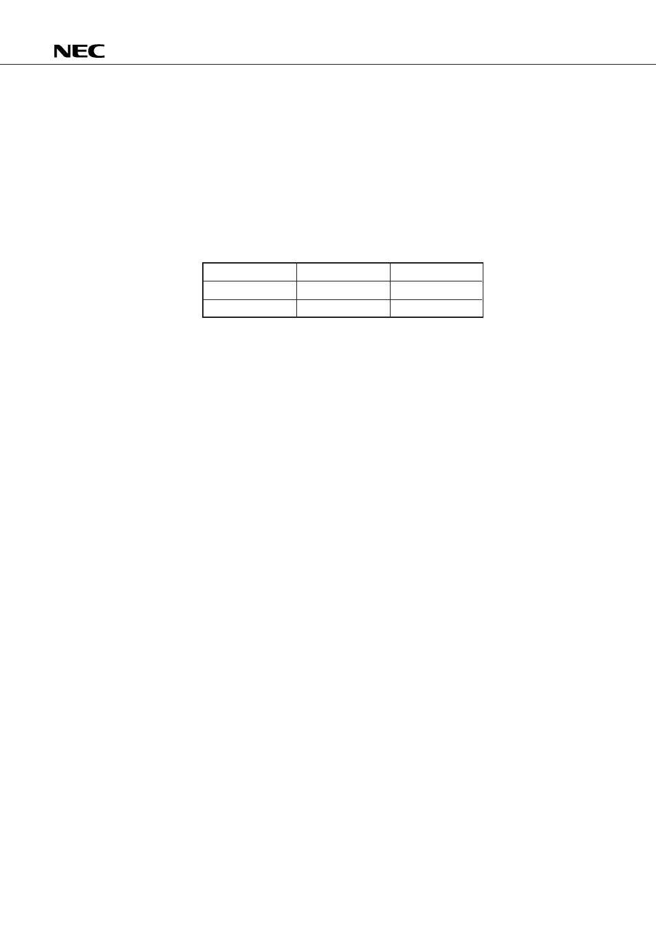
Table 20-6 CROM Bank
Remark The CROM bank should not be switched when the IDCEN flag is 1.
The register file at 30H can be read- and write-accessed, but the bits other than the CROMBNK flag (b
0
) are
always 0.
Because the CROM data is mapped in a program memory area, its size is 16 bits.
There are two types of CROM data.
(1) Character pattern data
(2) Control data
20.5.1 Character Pattern Data
The character pattern data is a character or graphic pattern. One character consists of 10 horizontal and
15 vertical dots. The corresponding character pattern data consists of 16 bits
×
15 steps. The data of 10
horizontal dots corresponds to one CROM step. 15 steps at addresses
××
0H to
××
EH in CROM form one
character pattern data item.
The structure of character pattern data varies according to whether the corresponding character has
rimming.
Fig. 20-6 shows the configuration of the character pattern data.
The highest bit selects whether there is rimming. Set the bit to 0 when the character has no rimming, when
the character has rimming, set the bit to 1.
For a character with no rimming, the lower 10 bits indicate the dot image of the actually displayed character
pattern. b
9
corresponds to the left section of the display, and b
0
to the right section. The bit that corresponds
to a bright dot is 1, and the bit that corresponds to a dark dot is 0.
For a character with rimming, the character pattern data is 5 bits as shown in Fig. 20-6. At this point, two
dots of the display pattern correspond to one character pattern data bit. This bit is combined with 10 rim data
bits (rim data is specified in one-dot units) to form a character pattern for a character with rimming.
With the 17K series assembler, the DCP pseudo instruction can define a character pattern easily. Use of
this instruction automatically generates the data shown in Fig. 20-6, regardless of whether there is rimming.
CROMBNK flag
CROM bank
CROM address
0
BANK0
0800H-0BFFH
1
BANK1
0C00H-0F7FH