4 power-on reset – NEC PD17062 User Manual
Page 177

177
µ
PD17062
14.4 POWER-ON RESET
Power-on reset is executed by raising V
DD
from a certain voltage (called the power-on clear voltage) or less.
When V
DD
is less than the power-on clear voltage, the power-on clear signal (POC) is output from the voltage
detection circuit shown in Fig. 14-1.
When the power-on clear signal is output, the crystal oscillation circuit stops and the device stops operating.
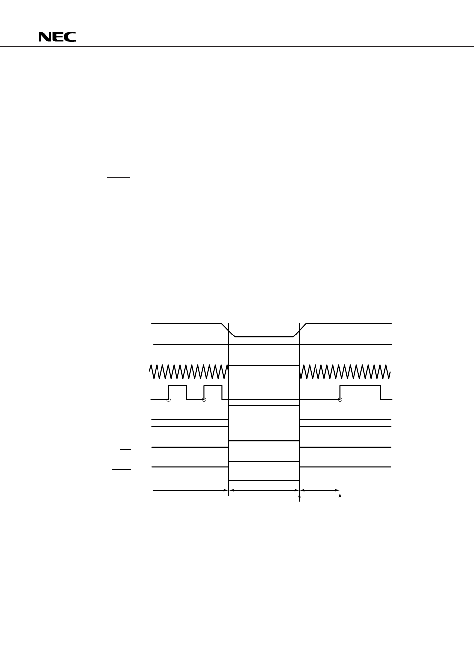
While the power-on clear signal is being output, the IRES, RES and RESET signals are output.
When V
DD
exceeds the power-on clear voltage, the power-on clear signal is dropped and crystal oscillation
starts. At the same time, the IRES, RES and RESET signals are also dropped.
Since the IRES signal halts release by timer carry FF, power-on reset is applied at the rising edge of the
next timer carry FF set signal.
Since the RESET signal has initialized the timer carry FF set signal to 100 ms, 50 ms after V
DD
exceeds the
power-on clear voltage, reset is applied and the program starts from address 0.
This operation is shown in Fig. 14-4.
At power-on reset, the program counter, stack, system register and control registers are initialized when
the power-on clear signal is output.
For the initial values, see the relevant items.
During normal operation, the power-on clear voltage is 3.5 V (rated value). In the clock-stop state, the
power-on clear voltage becomes 2.2 V (rated value).
Sections 14.4.1 and 14.4.2 describe operation at this time.
Section 14.4.3 describes operation when V
DD
rises from 0 V,
Fig. 14-4 Power-on Reset Operation
5 V
0 V
“H”
Normal operation
Device operation stopped
X
OUT
V
DD
CE
Timer carry FF
set pulse
IRES
RES
RESET
Reset signal
Power-on reset
Program starts from address 0
Power-on clear signal
Power-on clear release
Oscillation start
Halt state
50 ms
Power-on clear voltage
