Pll frequency synthesizer, 1 pll frequency synthesizer configuration – NEC PD17062 User Manual
Page 219

219
µ
PD17062
18. PLL FREQUENCY SYNTHESIZER
18.1 PLL FREQUENCY SYNTHESIZER CONFIGURATION
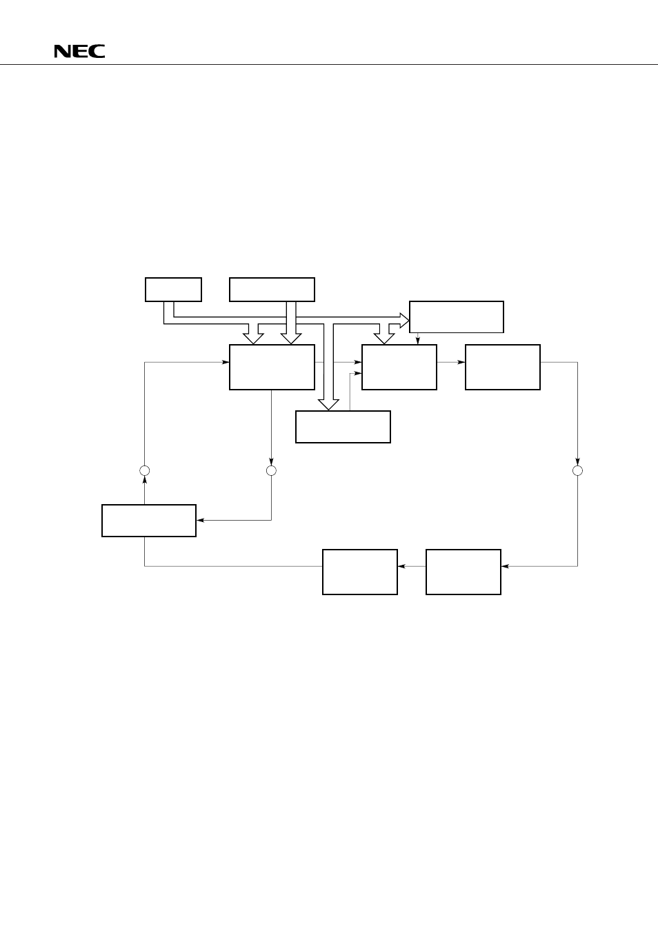
Fig. 18-1 is a block diagram of the PLL frequency synthesizer.
As shown in Fig. 18-1, the PLL frequency synthesizer consists of a programmable divider (PD), phase
comparator (
φ
-DET), reference frequency generator (RFG), and charge pump. Strictly speaking, a PLL
frequency synthesizer is configured by connecting these blocks with an external lowpass filter (LPF) and
voltage-controlled oscillator (VCO).
See Sections 18.3 to 18.5 for details of these blocks.
Fig. 18-1 PLL Frequency Synthesizer Block Diagram
Note External circuit
VCO
PSC
EO
Register
Data buffer
Unlock detection
block
Programmable
divider (PD)
Phase
comparator
( -DET)
φ
Charge pump
Reference frequency
generator (RFG)
Prescaler
P B595
Note
Note
Voltage-controlled
oscillator (VCO)
Lowpass filter
(LPF)
Note
µ
