3 bank register (bank), 4 memory pointer enable flag (mpe) – NEC PD17062 User Manual
Page 56
56
µ
PD17062
8.3 BANK REGISTER (BANK)
The bank register specifies a data memory bank.
The bank register contains BANK0 upon reset. The two high-order bits of address 79H are consistently set
to 0.
Data memory is classified into three banks by the bank register. When a data memory manipulation
instruction is executed, it acts on the data memory in the bank specified by the bank register.
For example, to manipulate BANK1 data memory with BANK0 set as the current bank, the bank must first
be switched to BANK1 in the bank register.
However, system registers allocated to addresses 74H-7FH of data memory are not confined to the concept
of banks. The same system registers exist at addresses 74H-7FH of all banks. Executing MOV 78H, #0 in BANK1
and MOV 78H, #0 in BANK2 both result in writing 0 to address 78H of the system register. Therefore, system
register manipulation is not constrained to the concept of banks.
When an interrupt is accepted, BANK is saved.
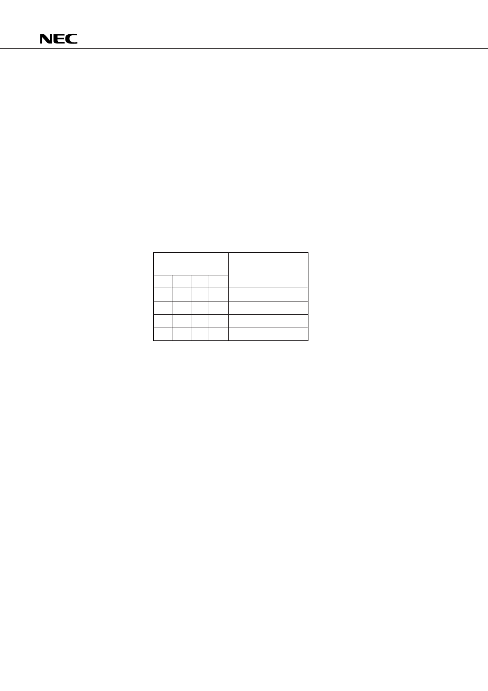
Table 8-1 Specification of Data Memory Bank
8.4 MEMORY POINTER ENABLE FLAG (MPE)
The MPE specifies whether to specify the row address for execution of the MOV @r, M and MOV M, @r
instructions by the MPL, or to perform execution with the same address. When the MPE is set, the row address
is specified by the MPL. When the MPE is reset, the instruction is executed with same row address.
However, the address specified by the MPL is the row address of the currently specified bank.
Bank request
Data memory bank
(BANK)
b
3
b
2
b
1
b
0
0
0
0
0
BANK0
0
0
0
1
BANK1
0
0
1
0
BANK2
0
0
1
1
Not to be set