NEC PD17062 User Manual
Page 165
165
µ
PD17062
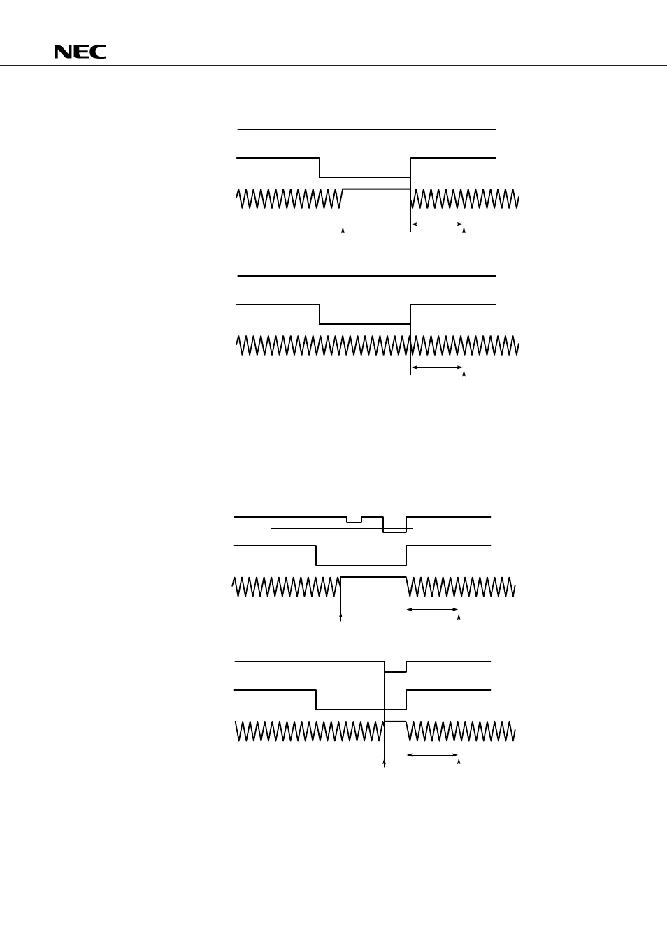
Fig. 13-4 Releasing the Clock Stop State by a CE Reset
Fig. 13-5 Releasing the Clock Stop State by a Power-on Reset
5 V
0 V
V
DD
CE pin
Crystal oscillation
(X
OUT
pin)
STOP 0 instruction
Approx. 50 ms
Program starts at address 0
(CE reset)
5 V
0 V
V
DD
CE pin
Clock oscillation
(X
OUT
pin)
If a clock-stop instruction is not used, operation is as follows:
0-t
SET
Program starts at address 0
(CE reset)
CE reset is applied in synchronization
with the setting of the timer carry FF
after the CE pin has been raised to high level.
5 V
0 V
V
DD
CE pin
Crystal oscillation
(X
OUT
pin)
STOP 0 instruction
Approx. 50 ms
Program starts at address 0
(CE reset)
5 V
0 V
V
DD
CE pin
Clock oscillation
(X
OUT
pin)
If a clock-stop instruction is not used, operation is as follows:
Approx. 50 ms
Program starts at address 0
(CE reset)
Oscillation stopped
3.5 V
2.2 V