NEC PD17062 User Manual
Page 70
70
µ
PD17062
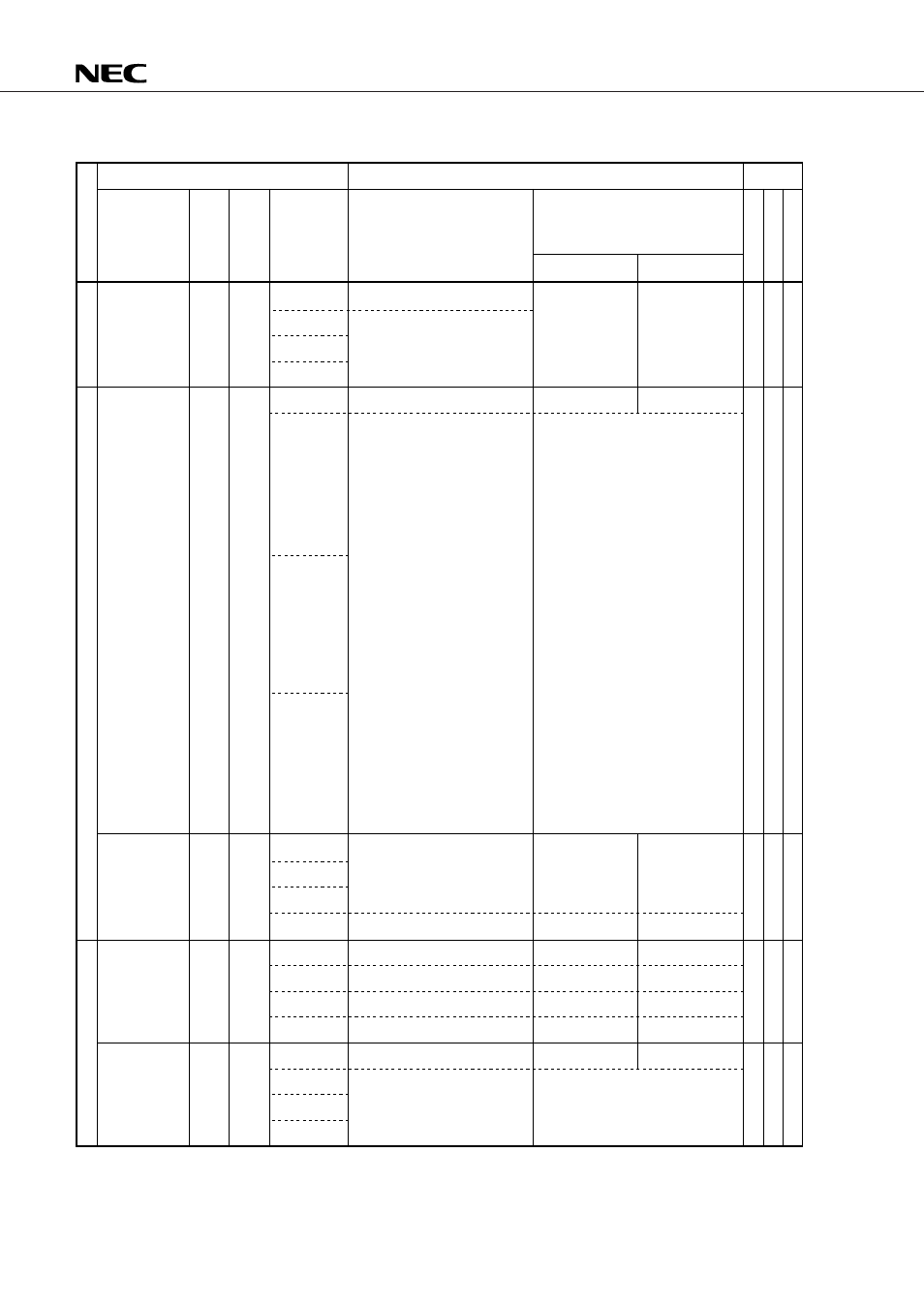
Table 9-1 Peripheral Hardware Control Functions of Control Registers (1/5)
Remark *: Retains the previous state.
Peripheral hardware
Control register
Peripheral hardware control function
At reset
Stack
Timer
Interrupt
Register
Ad-
dress
Read/
write
b3
b2
b1
b0
Symbol
Function outline
Set value
0
1
7
7
7
Stack pointer
(SP)
01H
R/W
0
(SP2)
(SP1)
(SP0)
Fixed at 0
Stack pointer
(3 bits are valid.)
BTM0ZX
On/off of zerocross circuit
BTM0CK2
BTM0CK0
0
0
0
BTM0CY
0
INTVSYN
0
INTNC
0
INTNCMD2
INTNCMD1
INTNCMD0
09H
R/W
17H
R
0FH
R
15H
R/W
Timer 0
clock select
register
BTM0CK1
Basic timer 0
carry flip-flop
judge register
Interrupt-level
judge register
INT
NC
mode
select register
Base clock setting of basic
timer 0 (internal/external)
Fixed at 0
Detects the carry flip-flop state
Fixed at 0
Detects the V
SYNC
pin state
Fixed at 0
Detects the INT
NC
pin state
Fixed at 0
Selects the pulse width of
interrupt accept pulse width
of the INT
NC
pin
No operation
Operation
Pulse for timer carry flop-flop set
0: 10 Hz (100 ms, internal)
1: 200 Hz (5 ms, internal)
2: 10 Hz (100 ms, internal)
3: 200 Hz (5 ms, internal)
4: f
TMIN
/5 Hz (external)
5: 200 Hz (5 ms, internal)
6: f
TMIN
/6 Hz (external)
7: 200 Hz (5 ms, internal)
Pulse for timer interrupt
0: 200 Hz (5 ms, internal)
1: 10 Hz (100 ms, internal)
2: 50 Hz (20 ms, internal)
3: 50 Hz (20 ms, internal)
4: 200 Hz (5 ms, internal)
5: f
TMIN
/5 Hz (external)
6: 200 Hz (5 ms, internal)
7: f
TMIN
/6 Hz (external)
0
0
*
0
1
1
0
0
0
0
0
0
Reset
Set
Low level
High level
Low level
High level
0: Accepts with edge
1: 200
s 2: 400 s 3: 2 ms
4: 4 ms
µ
µ
P
o
w
e
r
O
n
S
T
O
P
C
E