NEC PD17062 User Manual
Page 51
51
µ
PD17062
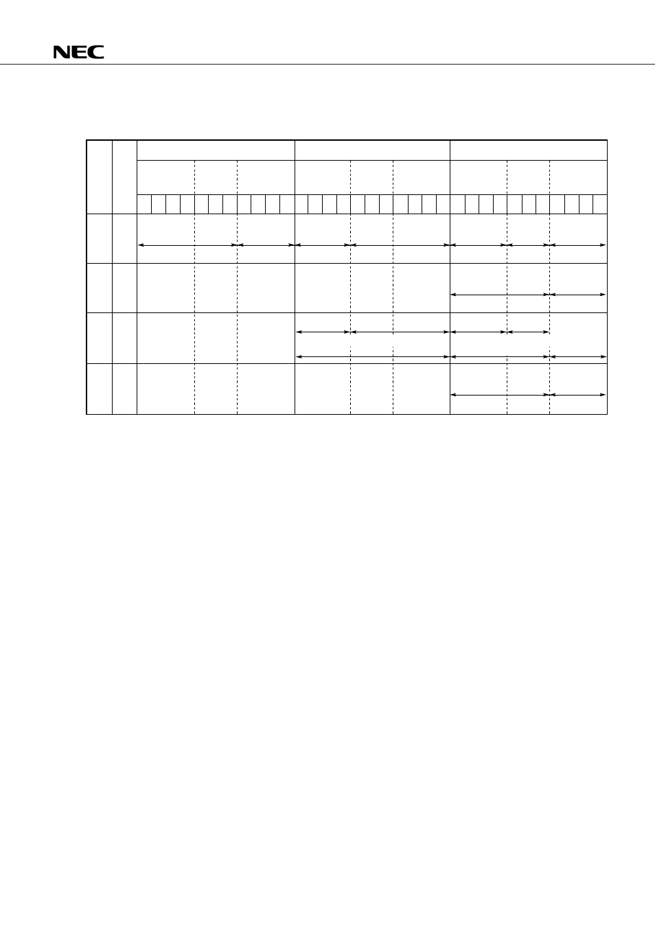
Table 7-2 Modification of the Data Memory Address and Indirect Transfer Address by the Index Register
and Data Memory Row Address Pointer
BANK
: Bank register
IX
: Index register
IXE
: Index enable flag
IXH
: Bits 10 to 8 of the index register
IXM : Bits 7 to 4 of the index register
IXL
: Bits 3 to 0 of the index register
m
: Data memory address specified with m
R
and m
C
m
R
: Data memory row address (high order)
m
C
: Data memory column address (low order)
MP
: Data memory row address pointer
MPE : Memory pointer enable flag
r
: General-purpose register column address
RP
: General-purpose register pointer
(
×
)
: Contents addressed by
×
b
3
b
2
b
1
b
0
b
2
b
1
b
0
b
3
b
2
b
1
b
0
b
3
b
2
b
1
b
0
b
2
b
1
b
0
b
3
b
2
b
1
b
0
b
3
b
2
b
1
b
0
b
2
b
1
b
0
b
3
b
2
b
1
b
0
IXE
MPE
0
0
0
1
1
0
1
1
RP
r
BANK
m
BANK
m
R
(r)
(r)
MP
BANK
m
BANK
m
R
(r)
MP
(r)
IXH, IXM
IX
Logical
OR
General-purpose register address
specified with r
Data memory address specified with m
Indirect transfer address specified with @r
Bank
Row
address
Column
address
Bank
Row
address
Column
address
Bank
Row
address
Column
address
Same as
above
Same as
above
Same as
above
Same as
above
Same as
above
Logical
OR