Serial interface, 1 serial interface mode register – NEC PD17062 User Manual
Page 201

201
µ
PD17062
16. SERIAL INTERFACE
The
µ
PD17062 has two sets of serial interface pins, channel 0 (CH0) and channel 1 (CH1), for exchanging
data with an external unit.
The CH0 pin, which consists of two wires, SDA and SCL, can be operated in any of three modes, clock
synchronous two-wire serial input, clock synchronous two-wire serial output, and two-wire bus
Note
. The SDA
and SCL pins can be used as general-purpose ports when not being used as a serial interface.
The CH1 pin, which consists of three wires, SCK, SO, and SI, can be operated in any of three modes, clock
synchronous two-wire serial I/O input, clock synchronous two-wire serial I/O output, and three-wire serial I/
O.
CH0 and CH1 cannot be operated at the same time. Which of pins CH0 and CH1 is used is specified with
the SIO0CH flag (register file: 08H, b
3
) of SMODE (Serial Interface Mode Register).
The two-wire hardware-supported bus mode is for the single master. Therefore, this mode does not support
any arbitration function. Arbitration must be done by the software.
Note The two-wire bus mode can be used as an I
2
C bus.
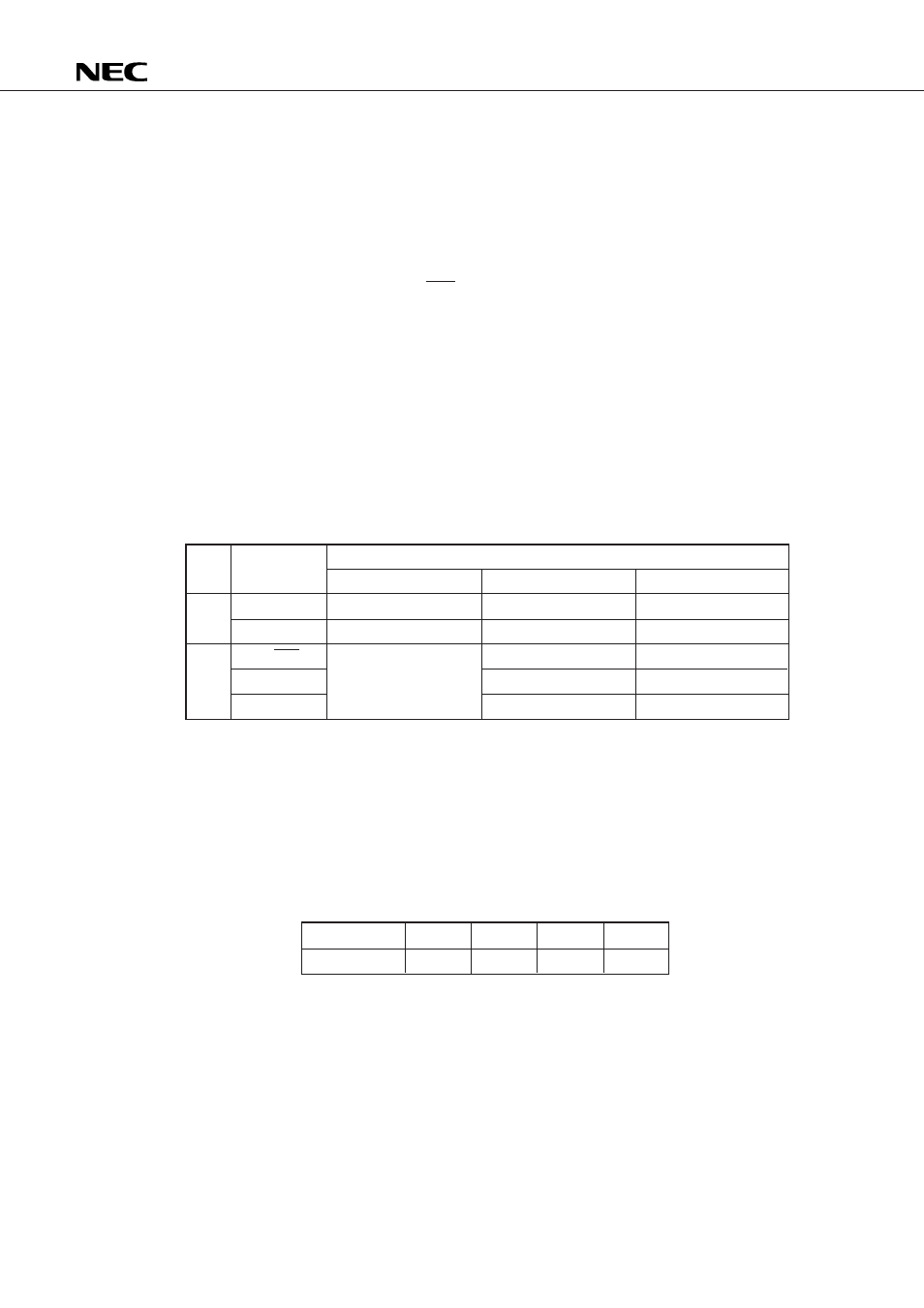
Table 16-1 External Pins for Serial Interface
16.1 SERIAL INTERFACE MODE REGISTER
The serial interface mode register specifies the operation mode of the serial interface. This register sets
up the channel to be used, the protocol, clock, and transmission/reception.
This register is mapped to address 08H in the register file.
All flags of this register are set to 0 at power-on reset.
Fig. 16-1 Configuration of Serial Interface Mode Register
CH
Pin name
Function
Two-wire bus mode
Serial I/O mode
Port I/O setting register
0
P0A
0
/SDA
Serial data I/O
Serial data I/O
P0ABIO0
P0A
1
/SCL
Shift clock I/O
Shift clock I/O
P0ABIO1
1
P0A
2
/SCK
Cannot be used
Shift clock I/O
P0ABIO2
P0A
3
/SO
Serial data output
P0ABIO3
P0B
0
/SI
Serial data input
P0BBIO0
Bit position
b
3
b
2
b
1
b
0
Flag name
SIO0CH
SB
SIO0MS
SIO0TX
