NEC PD17062 User Manual
Page 39
39
µ
PD17062
Example 2.
5.3.2 Notes on Using Unmounted Data Memory
As shown in Fig. 5-6, nothing is actually assigned to bit 0 (LSB) of address 72H of BANK1 of the port registers.
If a data memory manipulation instruction is executed for this address, the following operations are
performed:
(1) Device behavior
If a read instruction is executed, a 0 is read.
Executing a write instruction results in no change.
(2) Assembler behavior
Normal assembly is performed.
No error occurs.
(3) Emulator (IE-17K) behavior
If a read instruction is executed, a 0 is read.
Executing a write instruction results in no change.
No error occurs.
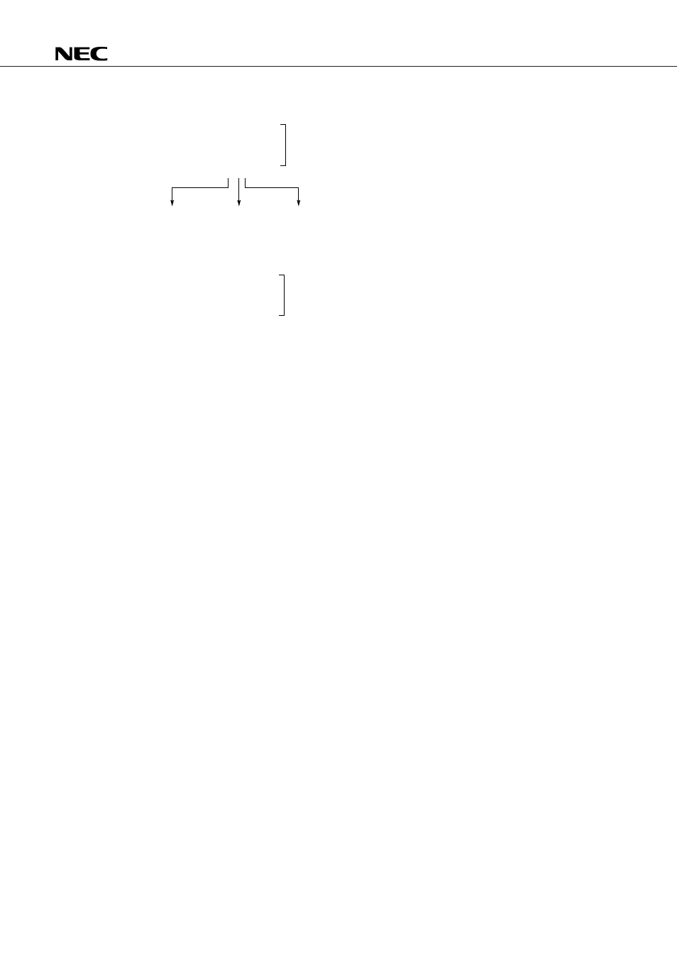
M1
M2
M3
MEM
MEM
MEM
0.15H
1.15H
2.15H
;
;
;
Bank
Row address
Column address
BANK1
MOV M1,
MOV M2,
MOV M3,
#0000B
#0000B
#0000B
;
;
;
;
Assembler built-in macro instruction BANK
←
1
M1, M2, and M3 are defined symbolically in
# for different
banks, but are for BANK1 in this program. Thus, all of these
three instructions write 0s to data memory address 15H in BANK1.
Symbol definition pseudo instruction