3 output circuit signal allocation, 3 outpu, 3 output circuit signal allocation -26 – Yaskawa SGDS Sigma III Servo Amplifier User Manual
Page 215
7 Operation
7.5.3 Output Circuit Signal Allocation
7-26
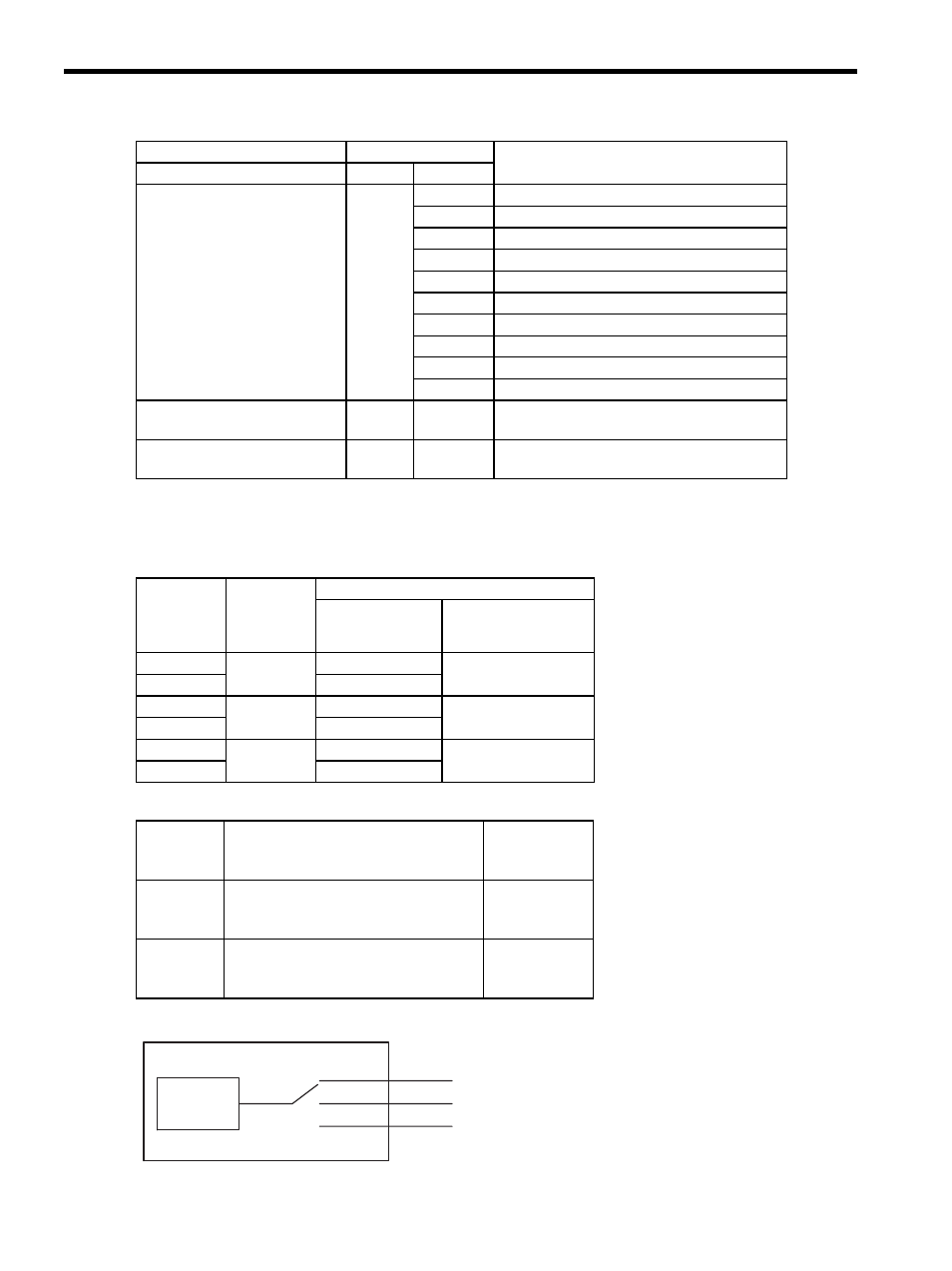
7.5.3 Output Circuit Signal Allocation
Output signal functions can be allocated to the sequence signal output circuits shown below.
In general, allocate signals according to the standard settings in the following table.
The output signal selection parameters and their factory settings are shown below.
Select the CN1 connector terminals that will output the signals.
External Latch Signal 1
(/EXT1)
Pn511.1
0 to 3
Sets signal OFF
4
ON when CN1-10 input signal is ON (L-level)
5
ON when CN1-11 input signal is ON (L-level)
6
ON when CN1-12 input signal is ON (L-level)
7
Sets signal ON
8
Sets signal OFF
D
ON when CN1-10 input signal is OFF (H-level)
E
ON when CN1-11 input signal is OFF (H-level)
F
ON when CN1-12 input signal is OFF (H-level)
9 to F
Sets signal OFF
External Latch Signal 2
(/EXT2)
Pn511.2
0 to F
Same as above.
External Latch Signal 3
(/EXT3)
Pn511.3
0 to F
Same as above.
Input Signal
Parameter
Description
Name
Number
Setting
CN1
Connector
Terminal
Numbers
Output
Terminal
Name
Factory Setting
Symbol
Name
1
SO1
/BK+(/SO1+)
General-purpose signal
output 1
2
/BK-(/SO1-)
23
SO2
/SO2+
General-purpose signal
output 2
24
/SO2-
25
SO3
/SO3+
General-purpose signal
output 3
26
/SO3-
Pn50E
Output Signal Selections 1
Factory
Setting:
0000
Pn50F
Output Signal Selections 2
Factory
Setting:
0100
Pn510
Output Signal Selections 3
Factory
Setting:
0000
1
2
3
Output
signal
SO1(CN1-1, 2)
SO2(CN1-23, 24)
SO3(CN1-25, 26)
Pn50E.
to Pn510.