1 mpc8548 memory map, Table 4-1, Mpc8548 features – Artesyn ATCA-9305 User's Manual (May 2014) User Manual
Page 93: Management complex
Management Complex
ATCA-9305 User’s Manual (10009109-07)
93
The MPC8548 processor has the following features:
For more detailed information, reference the Freescale MPC8548E PowerQUICC™ III Integrated
Processor Family Reference Manual.
4.1.1
MPC8548 Memory Map
The monitor can boot from either the soldered flash (Bank 1, default) or the socketed PLCC
device. Based on the configuration header (see
) either the
socketed device or soldered flash is mapped to the boot bank at FFF8, 000016, see
.
Information on particular portions of the memory map can be found in later sections of this
manual, see
.
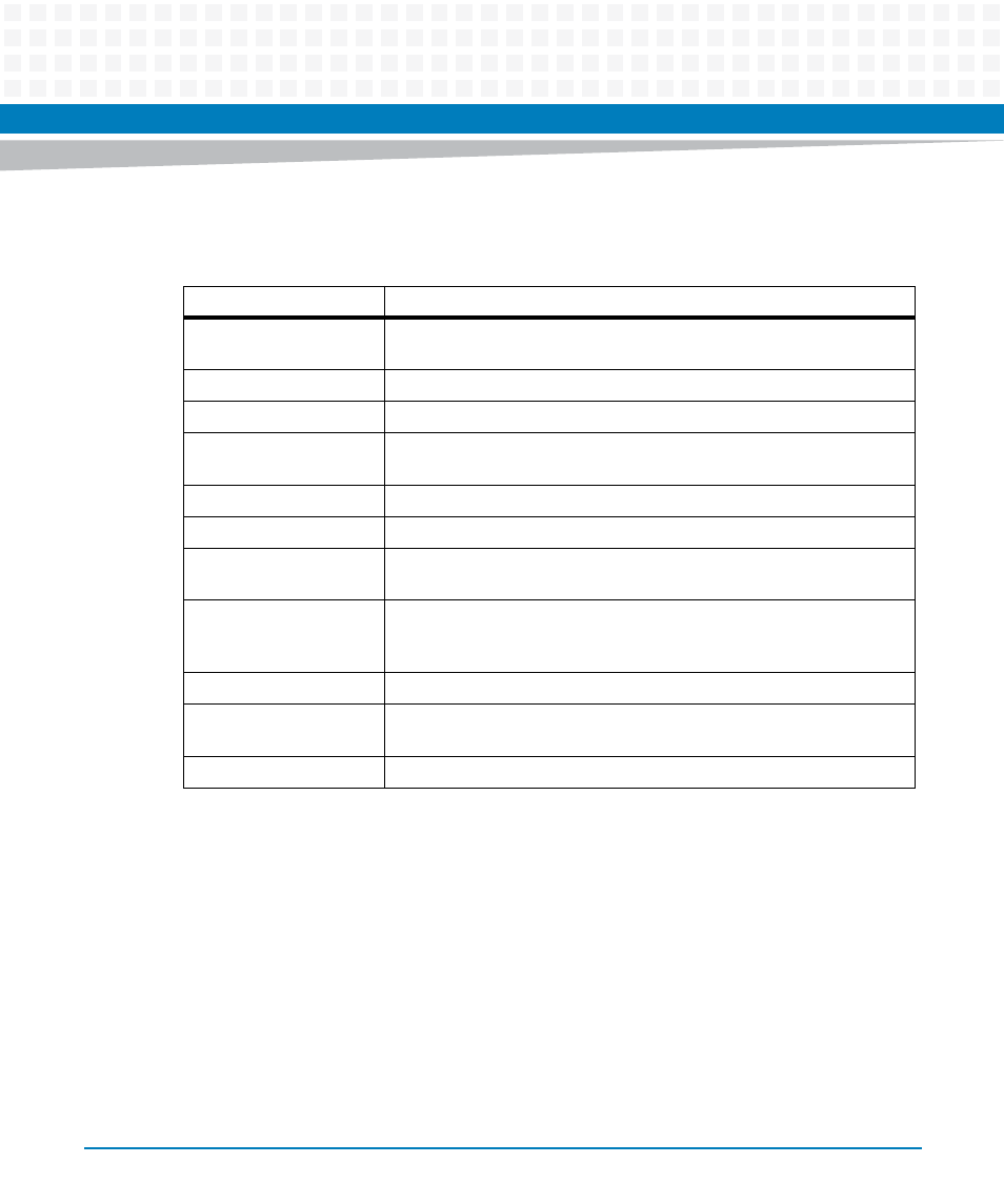
Table 4-1 MPC8548 Features
Feature
Description
L1 Cache
32-kilobyte data and instruction caches with parity protection, 32-byte
line, eight-way set associative
L2 Cache
512 kilobytes, eight-way set associative
CPU Core Speed
1 GHz with a 400 MHz DDR2 bus
DDR2 Memory Controller 64-bit data interface, four banks of memory supported (each up to 4 GB),
full ECC support
Dual I2C Controllers
Two-wire interface, master or slave I
2
C support
Boot Sequencer
Loads configuration data from serial ROM at reset via the I
2
C interface
Ethernet
Four 10/100/1000 enhanced three-speed controllers (eTSECs), full-/half-
duplex support, MAC address recognition
Local Bus Controller (LBC) DDR2 SDRAM memory controller, General Purpose Chip Select Machine
(GPCM), three User-Programmable Machines (UPM), eight chip selects
support eight external slaves
PCI
64-bit, PCI 2.2 compatible
PCI Express
Single x4 PCIe high-speed interconnect, complies with PCI Express™ Base
Specification Revision 1.0a
JTAG
Complies with IEEE Std. 1149.1