Delta Electronics Elevator Drive VFD-VL User Manual
Page 224
Appendix B Accessories|
Revision Nov. 2008, VLE1, SW V1.03
B-27
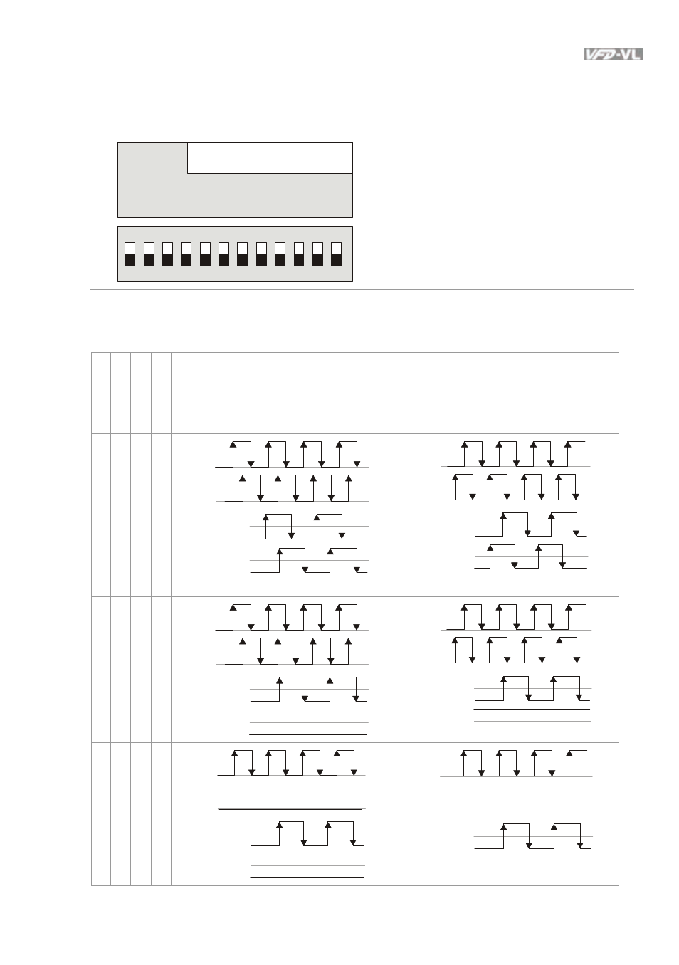
4. Output Signal Setting of the Frequency Divider
It generates the output signal of division factor
“n” after dealing with the input pulse. Please
set by the switch SW1 on the card.
ON
1 2 3 4 5 6 7 8 9 10 11 12
R
E
SERVE
I/
MO
DE
O/
M
O
D
E
RS
T
Division Factor
BI
T
0
BI
T
1
BI
T
2
BI
T
3
BI
T
4
BI
T
5
BI
T
6
BI
T
7
0
1
RESERVE: reserved bit (PIN1)
I/MODE: input type setting of the division
pulse (PIN 2)
O/MODE: output type setting of the division
pulse (PIN 3)
RST: clock reset bit (PIN 4)
Division factor: setting for division factor n:
1~256 (PIN5~12)
Settings and explanations
Division factor
RESE
RVE
I/M
O
D
E
O/MO
DE
RST
A leads B
B leads A
X 0 0 1
A-/A
B-/B
A/O-/A/O
B/O-/B/O
A-/A
B-/B
A/O-/A/O
B/O-/B/O
A/O-/A/O
B/O-/B/O
X 0 1 1
A-/A
B-/B
A/O-/A/O
B/O-/B/O
A/O-/A/O
B/O-/B/O
A-/A
B-/B
A/O-/A/O
B/O-/B/O
A/O-/A/O
B/O-/B/O
X 1 X 1
A-/A
B-/B
A/O-/A/O
B/O-/B/O
A/O-/A/O
B/O-/B/O
A-/A
B-/B
A/O-/A/O
B/O-/B/O
A/O-/A/O
B/O-/B/O
- 1x9 Bi-Directional Transceiver Module OPBD-155F2J1R (7 pages)
- Single Mode SFP Transceiver LCP-1250B4MDRx (14 pages)
- LC-1250xxxx Series (10 pages)
- Human Machine Interface DOP-AS Series (329 pages)
- Analog Output Module DVP04DA-S (2 pages)
- DeviceNet Slave Communication Module IFD9502 (2 pages)
- LCP-155B4MSRx (12 pages)
- High-Speed PCI 12-Axis Motion Control Card PCI-DMC-B01 (528 pages)
- Network Device DVP01PU-S (2 pages)
- GBIC-1250D5MR (12 pages)
- SPBD-1250A4Q1RT (10 pages)
- SILM4015 (1 page)
- LCP-8500A4EDR (14 pages)
- 10GBASE-SR SFP+ Optical Transceiver LCP-10G3A4EDR (16 pages)
- LCP-155A4HSRx (11 pages)
- LCP-1250RJ3SR-L (9 pages)
- SILM320L (1 page)
- LCP-1250RJ3SR-S (9 pages)
- SIL530 (1 page)
- Extension Digital I/O Module DOP-EXIO28RAE (1 page)
- DVP Series PLC DVP04TC-H2 (2 pages)
- 1x9 Bi-Directional Transceiver Module OPBD-155F1J1R (7 pages)
- Distribution Box TAP-CN01/02/03 (2 pages)
- LCP-200A4HSR (9 pages)
- Pulse Generation Unit DVP01PU-H2 (2 pages)
- Power Connection Interface VFD-PSD01 (1 page)
- Programmable Logic Controller DVP04DA-H2 (2 pages)
- Single Mode SFP Transceiver LCP-1250B4QDRx (13 pages)
- LCP-155B4JSRx Series (12 pages)
- Series Temperature Controller DTD Series (2 pages)
- Brake Modules BUE Series (2 pages)
- PLC DVP Series DVP-SX (2 pages)
- Digital Keypad / Display ASD-PU-01A (1 page)
- Multimode SFP Transceiver LCP-1250A4FDRx (14 pages)
- HMU1362M (1 page)
- RPA-01 (1 page)
- THMR1395 (1 page)
- SFBD-155F2J1RM (7 pages)
- Program Transfer Module DVP-PCC01 (1 page)
- RTU-DNET (41 pages)
- AC Servo Drive ASDA-AB (37 pages)
- Digital Keypad / Display ASD-PU-01B (1 page)
- HMR1045 (1 page)
- CANopen Communication Module DVPCOPM-SL (2 pages)
- SPBD-1250B4Q1R (10 pages)