7 dc dirty/valid region top (dc_dv_top), 02ch, Dc dirty/valid region top (dc_dv_top) – AMD Geode LX [email protected] User Manual
Page 324: 00000000h
324
AMD Geode™ LX Processors Data Book
Display Controller Register Descriptions
33234H
6.6.4.6
DC Video V Buffer Start Address Offset (DC_VID_V_ST_OFFSET)
This register specifies the offset at which the video V buffer starts.
Settings written to this register do not take effect until the start of the following frame or interlaced field.
6.6.4.7
DC Dirty/Valid Region Top (DC_DV_TOP)
This register specifies the top of the frame buffer memory region to be watched for frame-dirty mode.
Settings written to this register take effect immediately.
DC_VID_U_ST_OFFSET Bit Descriptions
Bit
Name
Description
31:28
FRAME_COUNT
Frame Count. When reading this register, this field indicates the current frame count, as
determined by counting rising edges of VIP VSYNC. This value is reset to 0 when
VIP_VSYNC occurs and FRAME_CNT >= FRAME_LIMIT. It can also be written to pro-
vide a mechanism for software to synchronize activities between the VIP and the Dis-
play Controller. However, this can result in corrupted video data until the next reset of
this counter.
27:0
OFFSET
Video U Buffer Start Offset. This value represents the starting location for the Video U
Buffer. The lower three bits should always be programmed as zero so that the start off-
set is aligned to a QWORD boundary. A buffer for U data is only used if YUV 4:2:0 dis-
play mode is selected (DC Memory Offset 004h[20] = 1).
DC Memory Offset 028h
Type
R/W
Reset Value
xxxxxxxxh
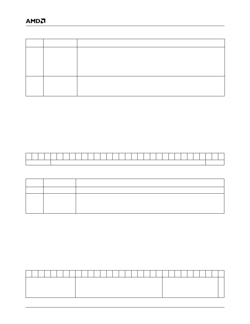
DC_VID_V_ST_OFFSET Register Map
31 30 29 28 27 26 25 24 23 22 21 20 19 18 17 16 15 14 13 12 11 10
9
8
7
6
5
4
3
2
1
0
RSVD
OFFSET
0
DC_VID_V_ST_OFFSET Bit Descriptions
Bit
Name
Description
31:28
RSVD
Reserved.
27:0
OFFSET
Video V Buffer Start Offset. This value represents the starting location for the Video V
Buffer. The lower three bits should always be programmed as zero so that the start offset
is aligned to a QWORD boundary. A buffer for V data is only used if YUV 4:2:0 display
mode is selected (DC Memory Offset 004h[20] = 1).
DC Memory Offset 02Ch
Type
R/W
Reset Value
00000000h
DC_DV_TOP Register Map
31 30 29 28 27 26 25 24 23 22 21 20 19 18 17 16 15 14 13 12 11 10
9
8
7
6
5
4
3
2
1
0
RSVD
DV_TOP
RSVD
D
V
_T
OP_EN