15 glcp debug clock control (glcp_dbgclkctl), 16 chip revision id (glcp_chip_revid), Glcp debug clock control (glcp_dbgclkctl) – AMD Geode LX [email protected] User Manual
Page 559: 00000000_00000002h, 4c000017h, Chip revision id (glcp_chip_revid), 00000000_000000xxh
AMD Geode™ LX Processors Data Book
559
GeodeLink™ Control Processor Register Descriptions
33234H
6.14.2.15 GLCP Debug Clock Control (GLCP_DBGCLKCTL)
Note that after the mux to select the clock, a standard clock control gate exists. This register should never be changed from
one non-zero value to another. Always write this register to 0 when moving to an alternative debug clock.
6.14.2.16 Chip Revision ID (GLCP_CHIP_REVID)
MSR Address
4C000016h
Type
R/W
Reset Value
00000000_00000002h
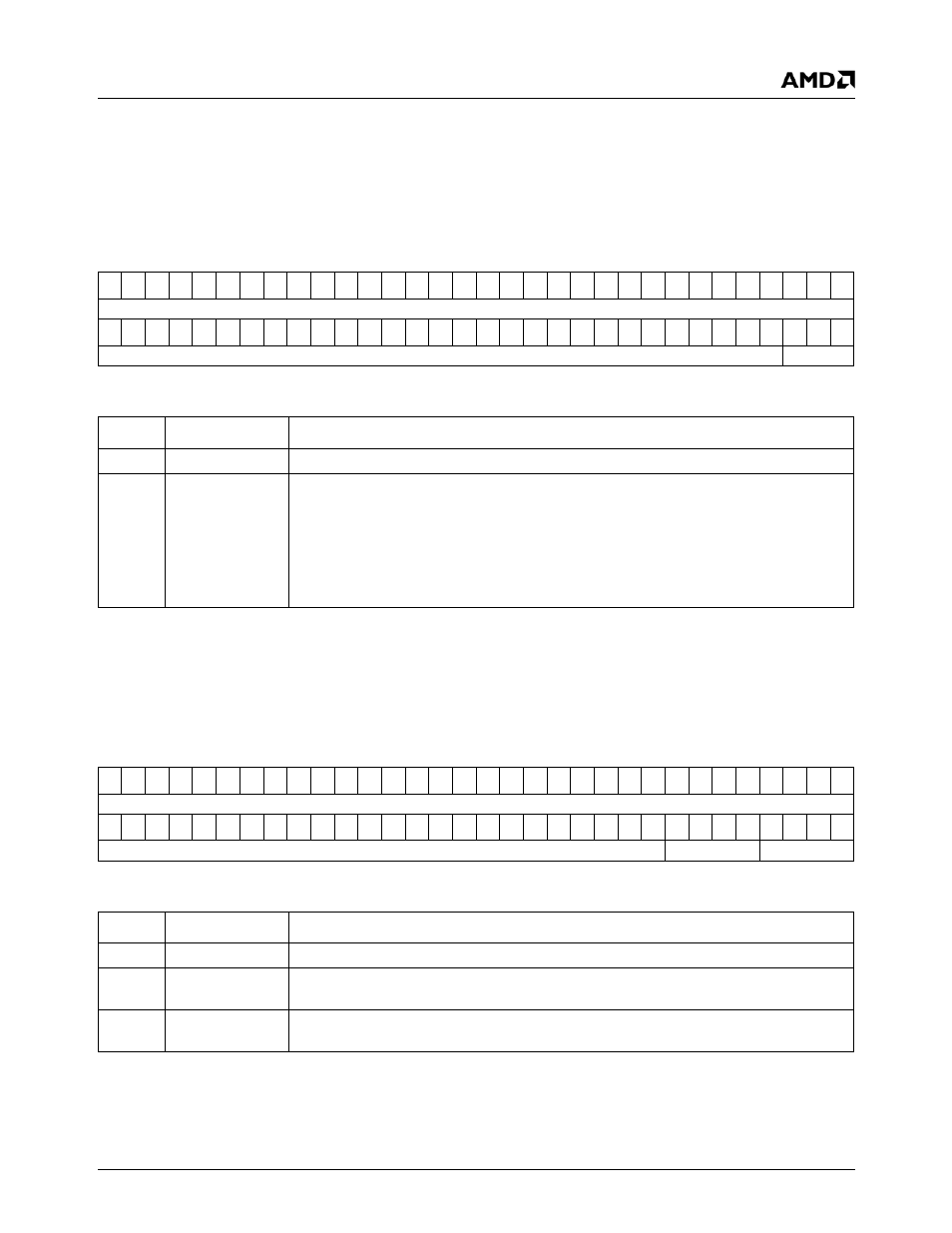
GLCP_DBGCLKCTL Register Map
63 62 61 60 59 58 57 56 55 54 53 52 51 50 49 48 47 46 45 44 43 42 41 40 39 38 37 36 35 34 33 32
RSVD
31 30 29 28 27 26 25 24 23 22 21 20 19 18 17 16 15 14 13 12 11 10
9
8
7
6
5
4
3
2
1
0
RSVD
CLKSEL
GLCP_DBGCLKCTL Bit Descriptions
Bit
Name
Description
63:3
RSVD
Reserved. Write as read.
2:0
CLKSEL
Clock Select. Selects the clock to drive into the debug logic.
000: None.
001: CPU Core clock.
010: GLIU1 clock.
011: DOTCLK.
100: PCI clock.
101-111: Reserved.
MSR Address
4C000017h
Type
RO
Reset Value
00000000_000000xxh
GLCP_CHIP_REVID Register Map
63 62 61 60 59 58 57 56 55 54 53 52 51 50 49 48 47 46 45 44 43 42 41 40 39 38 37 36 35 34 33 32
RSVD
31 30 29 28 27 26 25 24 23 22 21 20 19 18 17 16 15 14 13 12 11 10
9
8
7
6
5
4
3
2
1
0
RSVD
MAJ
MIN
GLCP_CHIP_REVID Bit Descriptions
Bit
Name
Description
63:8
RSVD
Reserved. Reads as 0.
7:4
MAJ
Major Revision. Identifies major silicon revision. See AMD Geode™ LX Processors
Specification Update document for value.
3:0
MIN
Minor Revision. Identifies minor silicon revision. See AMD Geode™ LX Processors
Specification Update document for value.