4 internal test and measurement interface signals – AMD Geode LX [email protected] User Manual
Page 36
36
AMD Geode™ LX Processors Data Book
33234H
DQM[7:0]
N30, H29,
C24, A19,
B10, A6,
G2, M1
I/O
166-400 Mb/s
2.5
Data Mask Control Bits. During memory read
cycles, these outputs control whether the
SDRAM output buffers are driven on the Mem-
ory Data Bus or not. All DQM signals are
asserted during read cycles.
During memory write cycles, these outputs con-
trol whether or not memory data is written into
the SDRAM.
DQM[0] is associated with MD[7:0].
DQM[7] is associated with MD[63:56].
DQ[63:0]
See Table
I/O
166-400 Mb/s
2.5
Memory Data Bus.
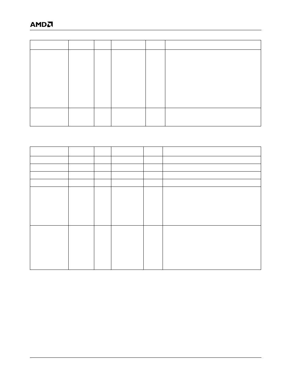
3.4.3
Memory Interface Signals (DDR) (Continued)
Signal Name
Ball No.
Type
f
V
Description
3.4.4
Internal Test and Measurement Interface Signals
Signal Name
Ball No.
Type
f
V
Description
TCLK
AC2
I
0-66 MHz
3.3
Test Clock. JTAG test clock.
TMS
AA4
I
0-66 Mb/s
3.3
Test Mode Select. JTAG test mode select.
TDI
AB3
I
0-66 Mb/s
3.3
Test Data Input. JTAG serial test data input.
TDO
AC1
O
0-66 Mb/s
3.3
Test Data Output. JTAG serial test data output.
TDBGI
AB2
I
0-400 Mb/s
3.3
Test Debug Input. The Debug Management
Interrupt (DMI) is input via TDBGI. The selects
for TDBGI are MSR programmable via the GLCP
module. When using TDBGI for DMI, it cannot be
used for other debug purposes. DMI can be
setup via the GLCP module to be edge sensitive
or level sensitive
TDBGO
AB4
O
(PD)
0-400 Mb/s
3.3
Test Debug Output. The AMD Geode LX pro-
cessor can output internal clocks on TDBGO.
The selects for TDBGO are MSR programmable
via the GLCP module. The internal clock can be
selected from any clock domain and may be
divided down by 2 or 3 before output. This
enables tester and board level visibility of the
internal clock quality.