AMD Geode LX [email protected] User Manual
Page 234
234
AMD Geode™ LX Processors Data Book
GeodeLink™ Memory Controller Register Descriptions
33234H
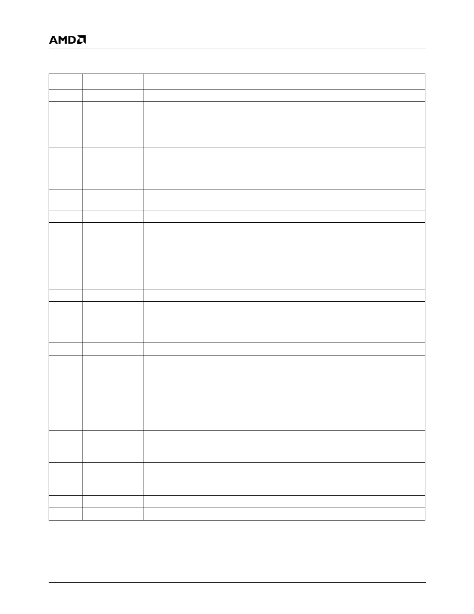
MC_CFCLK_DBUG Bit Descriptions
Bit
Name
Description
63:35
RSVD
Reserved.
34
B2B_DIS
Back-to-Back Command Disable. Setting this bit disables the issuing of DRAM com-
mands within back-to-back cycles in both MTEST and normal functional mode. To maxi-
mize performance, this should only be used in MTEST mode, where the cycle following
the command cycle should be idle for the logic analyzer to be able to properly capture
and interpret the MTEST data. (Default = 0) (back-to-back commands allowed).
33
MTEST_RBEX_
EN
MTEST RBEX Enable. Enables the outputting of read byte enables information on reads
with RBEXs.
0: Disable. (Default)
1: Enable.
32
MTEST_EN
MTEST Enable. Enables MTEST debug mode, which multiplexes debug data onto the 13
DRAM address output pins, one cycle after the command cycle. (Default = 0)
31:17
RSVD
Reserved.
16
FORCE_PRE
Force Precharge-all. Force precharge-all command before load-mode and refresh com-
mands, even when banks are already all closed. Normally, a precharge-all command only
gets issued conditionally before a load-mode or refresh command: only if the module
banks are not all closed yet. With this bit set, the precharge-all will be issued uncondition-
ally before the load-mode or refresh command.
0: Disable. (Default)
1: Enable.
15:13
RSVD
Reserved.
12
TRISTATE_DIS
TRI-STATE Disable.This bit controls the power saving feature that puts the GLMC's
address and control pins into TRI-STATE mode during idle cycles or during PMode1.
0: Tri-stating enabled.
1: Tri-stating disabled. (Default)
11:10
RSVD
Reserved.
9:8
MASK_CKE[1:0]
CKE Mask. Mask output enables for CKE[1:0]. After power-up or warm reset, software
can complete all necessary initialization tasks before clearing this mask to allow commu-
nication with the DRAM. These bits can also be used to selectively mask off the CKE sig-
nal of a DIMM that is not installed.
00: CKE1 and CKE0 unmasked.
01: CKE1 unmasked, CKE0 masked.
10: CKE1 masked, CKE0 unmasked.
11: CKE1 and CKE0 masked. (Default)
7
CNTL_MSK1
Control Mask 1. Mask output enable bit for DIMM1’s CAS1#, RAS1#, WE1#, CS[3:2]#.
0: Unmasked. (Default)
1: Masked.
6
CNTL_MSK0
Control Mask 0. Mask output enable bit for DIMM0’s CAS0#, RAS0#, W0#, CS[1:0]#.
0: Unmasked. (Default)
1: Masked.
5
ADRS_MSK
Address Mask. Mask output enable bit for MA and BA. (Default = 0)
4:0
RSVD
Reserved.