9 gliu control registers, 1 dc gliu0 memory offset (dc_gliu0_mem_offset), 2 dc dirty/valid ram control (dc_dv_ctl) – AMD Geode LX [email protected] User Manual
Page 339: Dc gliu0 memory offset (dc_gliu0_mem_offset), Dc dirty/valid ram control (dc_dv_ctl)
AMD Geode™ LX Processors Data Book
339
Display Controller Register Descriptions
33234H
6.6.9
GLIU Control Registers
6.6.9.1
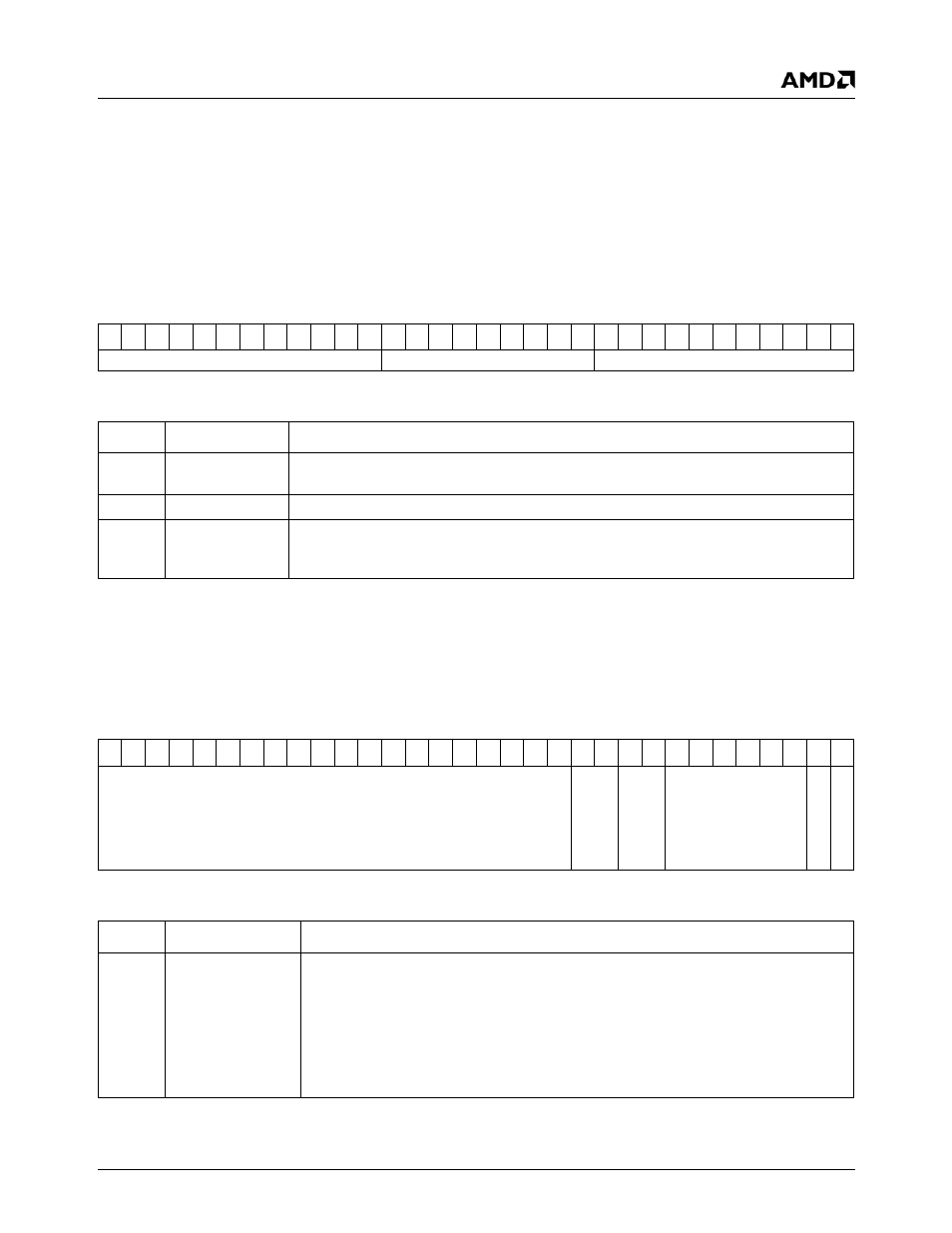
DC GLIU0 Memory Offset (DC_GLIU0_MEM_OFFSET)
This register is used to set a base address for the graphics memory region. The value in this register is added to all outgo-
ing memory addresses. Because the base address must be aligned to a 16 MB region, only bits [31:24] of this register are
used.
6.6.9.2
DC Dirty/Valid RAM Control (DC_DV_CTL)
DC Memory Offset 084h
Type
R/W
Reset Value
00000000h
DC_GLIU0_MEM_OFFSET Register Map
31 30 29 28 27 26 25 24 23 22 21 20 19 18 17 16 15 14 13 12 11 10
9
8
7
6
5
4
3
2
1
0
GLIU0_MEM_OFFSET
RSVD
DV_RAM_AD
DC_GLIU0_MEM_OFFSET Bit Descriptions
Bit
Name
Description
31:20
GLIU0_
MEM_OFFSET
GLIU0 Memory Offset. Base address (1 MB aligned) for the graphics memory region.
This value is added to all outgoing memory addresses.
19:11
RSVD
Reserved. Equal to 0.
10:0
DV_RAM_AD
DV RAM Address. This value is used to allow direct software access to the Dirty/Valid
(DV) RAM. The address must be written in this location before reading or writing the DV
RAM Access Register (DC Memory Offset 08Ch).
DC Memory Offset 088h
Type
R/W
Reset Value
00000000h
DC_DV_CTL Register Map
31 30 29 28 27 26 25 24 23 22 21 20 19 18 17 16 15 14 13 12 11 10
9
8
7
6
5
4
3
2
1
0
DV Address Offset
D
V
_LIN
E
_
S
IZ
E
DV
_
R
A
N
G
E
RSVD
DV
_
M
A
S
K
CL
E
A
R_
D
V
_
R
A
M
DV_CTL Bit Descriptions
Bit
Name
Description
31:12
DV Address
Offset
DV Address Offset. When the DV RAM observes memory transactions, the
addresses correspond to memory controller device address space. However, the DV
RAM is organized based on the internal DC device address space. To account for this,
the value indicated by this field is shifted to correspond to address bits [31:12], and
then subtracted from memory addresses before determining an offset into the DV
RAM. When programming the value in this field, software must calculate the sum of the
GLIU0_MEM_OFFSET (DC Memory Offset 084h[31:24] and the appropriate Physical-
to-Device descriptor(s) in GLIU0.