Figure 7-7, Table 7-11, Flat panel interface signals – AMD Geode LX [email protected] User Manual
Page 611
AMD Geode™ LX Processors Data Book
611
Electrical Specifications
33234H
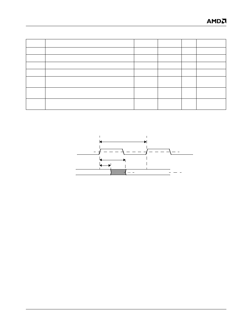
Figure 7-7. Drive Level and Measurement Points for Switching Characteristics
Table 7-11. Flat Panel Interface Signals
Symbol
Parameter
Min
Max
Unit
Comments
t
CK
DOTCLK period
6.0
ns
166 MHz
t
CH
DOTCLK High time
2.7
ns
45% t
CK
t
CL
DOTCLK Low time
2.7
ns
45% t
CK
DOTCLK long term output jitter
15%
t
CK
Note
1
t
VAL1
DRGB[31:0] Output Valid Delay time from rising
edge of DOTCLK
0.5
3.0
ns
t
VAL2
DISPEN, LDEMOD Output Valid Delay time from
rising edge of DOTCLK
0.5
3.0
ns
t
VAL3
HSYNC, VSYNC Output Valid Delay time from ris-
ing edge of DOTCLK
0.5
3.0
ns
Note 1. Measured as per VESA requirements. The jitter is observed at its worst case point on a scan line after HSYNC
triggers up to and including the next HSYNC trigger.
DOTCLK
Outputs
50%
Valid Output
n+1
Valid Output
n
50%
t
VAL1,2,3
Min
t
VAL1,2,3
Max
t
CK