2 display configuration (dcfg), Display configuration (dcfg) – AMD Geode LX [email protected] User Manual
Page 422
422
AMD Geode™ LX Processors Data Book
Video Processor Register Descriptions
33234H
6.8.3.2
Display Configuration (DCFG)
5
SC_BYP
Scaler Bypass. Bypass scaling math functions. Should only be used for non-scaled
video outputs. Scale factors set to 10000h.
0: Scaler enabled.
1: Scaler disabled.
4
RSVD (RO)
Reserved (Read Only). Reads back as 0.
3:2
VID_FMT
Video Format. Byte ordering of video data on the video input bus. The interpretation of
these bits depends on the settings for bit 28 (EN_420) and bit 13 (GV_SEL) of the VDE
register (VP Memory Offset 098h).
If GV_SEL and EN_420 are both set to 0 (4:2:2):
00: Cb Y0 Cr Y1
01: Y1 Cr Y0 Cb
10: Y0 Cb Y1 Cr
11: Y0 Cr Y1 Cb
If GV_SEL is set to 0 and EN_420 is set to 1 (4:2:0):
00: Y0 Y1 Y2 Y3
01: Y3 Y2 Y1 Y0
10: Y1 Y0 Y3 Y2
11: Y1 Y2 Y3 Y0
If GV_SEL is set to 1 and EN_420 is set to 0 (5:6:5):
00: P1L P1M P2L P2M
01: P2M P2L P1M P1L
10: P1M P1L P2M P2L
11: P1M P2L P2M P1L
Both RGB 5:6:5 and YUV 4:2:2 contain two pixels in each 32-bit DWORD. YUV 4:2:0
contains a stream of Y data for each line, followed by U and V data for that same line.
Cb = u, Cr = v.
1
RSVD (RO)
Reserved (Read Only). Reads back as 0.
0
VID_EN
Video Enable. Enables video acceleration hardware.
0: Disable (reset) video module.
1: Enable.
VP Memory Offset 008h
Type
R/W
Reset Value
00000000_00000000h
VCFG Bit Descriptions (Continued)
Bit
Name
Description
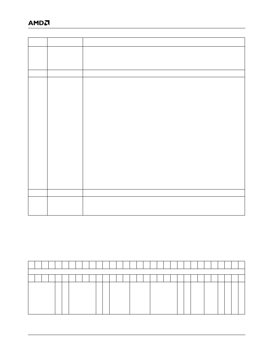
DCFG Register Map
63 62 61 60 59 58 57 56 55 54 53 52 51 50 49 48 47 46 45 44 43 42 41 40 39 38 37 36 35 34 33 32
RSVD
31 30 29 28 27 26 25 24 23 22 21 20 19 18 17 16 15 14 13 12 11 10
9
8
7
6
5
4
3
2
1
0
SP
RSVD
D
A
C_VREF
RSVD
GV
_G
A
M
VG
_
C
K
RSVD
CR
T
_
SYNC_SKW
SP
CR
T
_
VSYNC_POL
CR
T_HSYNC
_
PO
L
RSVD
SP
D
A
C
_
BL_EN
VS
YN
C_EN
HSYNC_
E
N
CR
T
_
E
N