AMD Geode LX [email protected] User Manual
Page 230
230
AMD Geode™ LX Processors Data Book
GeodeLink™ Memory Controller Register Descriptions
33234H
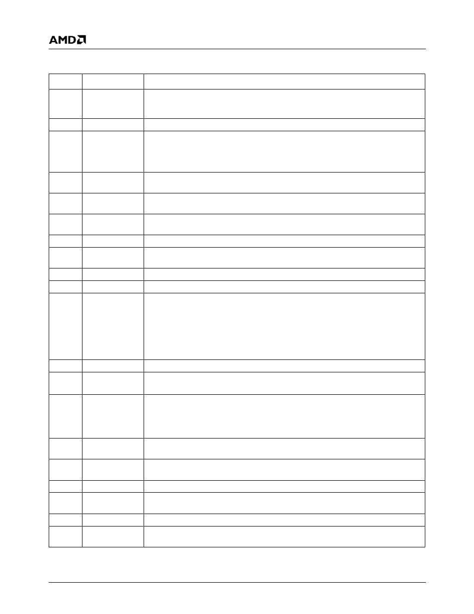
MC_CF8F_DATA Bit Descriptions
Bit
Name
Description
63:56
STALE_REQ
GLIU Max Stale Request Count. Non-high priority requests (PRI = 0) are made high-pri-
ority requests when the request is not serviced within max stale request count clocks.
(Default = 18h)
55:53
RSVD
Reserved.
52:51
XOR_BIT_SEL
XOR Bit Select. Selects which upper GLIU address bit to XOR with MB0, BA1 or BA0
(see "Auto Low Order Interleaving" on page 212). Only applies to LOI mode. (Default =
00).
00: ADDR[18] 01: ADDR[19] 10: ADDR[20] 11: ADDR[21]
50
XOR_MB0
XOR MB0 Enable. Enables XORing of module bank select MB0 with upper GLIU
address bit selected by XOR_BIT_SEL (bits [52:51]). (Default = 0, Disabled)
49
XOR_BA1
XOR BA1 Enable. Enables XORing of component bank select BA1 with upper GLIU
address bit selected by XOR_BIT_SEL (bits [52:51]). (Default = 0, Disabled)
48
XOR_BA0
XOR BA0 Enable. Enables XORing of component bank select BA0 with upper GLIU
address bit selected by XOR_BIT_SEL (bits [52:51]). (Default = 0, Disabled)
47:42
RSVD
Reserved.
41
TRUNC_DIS
Burst Truncate Disable. Disables truncation of read/write bursts. This disable reduces
performance and should only be used during debug. (Default = 0, bursts enabled)
40
REORDER_DIS
Reorder Disable. Disables the reordering of requests. This bit must be set to 1.
39:34
RSVD
Reserved.
33
HOI_LOI
High / Low Order Interleave Select (HOI / LOI). Selects the address interleaving mode.
HOI uses fixed upper address bits to map the GLIU address to a component bank. LOI
uses variable lower address bits depending on page size, number of module banks, and
number of component banks of the DIMMs, plus an option to XOR with upper address
bits.
1: HOI.
0: LOI. (Default)
32
RSVD
Reserved.
31
THZ_DLY
tHZ Delay. Add 1 extra clock on read-to-write turnarounds to satisfy DRAM parameter
t
HZ
for higher frequencies. (Default = 0)
30:28
CAS_LAT
Read CAS Latency. Number of clock delays between Read command and Data valid.
CAS Latency:
000: RSVD
010: 2 (Default)
100: 4
110: 2.5
001: RSVD
011: 3
101: 1.5
111: 3.5
27:24
ACT2ACTREF
ACT to ACT/REF Period. tRC. Minimum number of SDRAM clocks between ACTIVE
and ACTIVE/AUTO REFRESH commands. (Default = 8h)
23:20
ACT2PRE
ACT to PRE Period. tRAS. Minimum number of clocks from ACT to PRE commands on
the same component bank. (Default = 7h)
19
RSVD
Reserved.
18:16
PRE2ACT
Pre to Act Period. tRP. Minimum number of SDRAM clocks between PRE and ACT com-
mands. (Default = 011)
15
RSVD
Reserved.
14:12
ACT2CMD
Delay Time from Act To read/WRITE. tRCD. Minimum number of SDRAM clocks
between ACT and READ/WRITE commands. (6..2 valid). (Default = 011)