11 vip task a video pitch (vip_task_a_vid_pitch), 12 vip control register 3 (vip_contrl_reg3), Vip task a video pitch (vip_task_a_vid_pitch) – AMD Geode LX [email protected] User Manual
Page 498: 00000000h, Vip control register 3 (vip_contrl_reg3), 00000020h
498
AMD Geode™ LX Processors Data Book
Video Input Port Register Descriptions
33234H
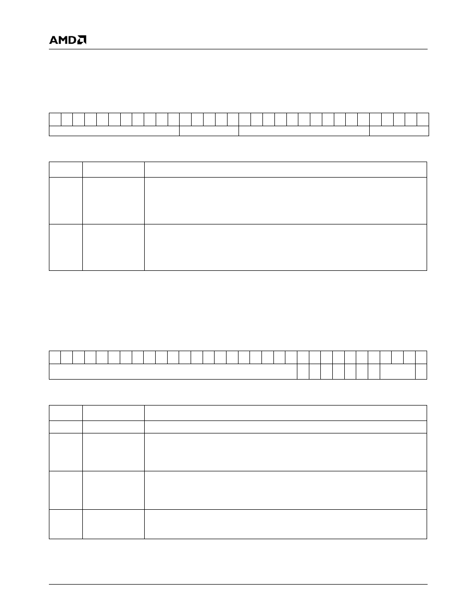
6.10.2.11 VIP Task A Video Pitch (VIP_TASK_A_VID_PITCH)
6.10.2.12 VIP Control Register 3 (VIP_CONTRL_REG3)
VIP Memory Offset 28h
Type
R/W
Reset Value
00000000h
VIP_TASK_A_VID_PITCH Register Map
31 30 29 28 27 26 25 24 23 22 21 20 19 18 17 16 15 14 13 12 11 10
9
8
7
6
5
4
3
2
1
0
TASK_A_UV_PITCH
Program to 00000
TASK_A_VIDEO_PITCH
Program to 00000
VIP_TASK_A_VID_PITCH Bit Descriptions
Bit
Name
Description
31:16
TASK_A_UV_
PITCH
Task A UV Pitch. Specifies the logical width of the video data buffer when in linear
mode. Specifies the logical width of the U and V buffers when in planar mode. This value
is added to the start of the line address to get the address of the next line where captured
video data will be stored. This value must be an integral number of QWORDs. This value
needs to be 32-byte aligned. (Bits [20:16] are required to be 00000.)
15:0
TASK_A_
VIDEO_PITCH
Task A Video Pitch. Specifies the logical width of the video data buffer when in linear
mode. Specifies the logical width of the Y buffer when in planar mode. This value is
added to the start of the line address to get the address of the next line where captured
video data will be stored. This value must be an integral number of QWORDs. This value
needs to be 32-byte aligned. (Bits [4:0] are required to be 00000.)
VIP Memory Offset 2Ch
Type
R/W
Reset Value
00000020h
VIP_CONTRL_REG3 Register Map
31 30 29 28 27 26 25 24 23 22 21 20 19 18 17 16 15 14 13 12 11 10
9
8
7
6
5
4
3
2
1
0
RSVD
PDM
BR
U
DOR
EFD
TP
VP
HP
RSVD
FR
VIP_CONTRL_REG3 Bit Descriptions
Bit
Name
Description
31:11
RSVD
Reserved.
10
PDM
Planar De-interlace Mode. When set to 1, the U/V even buffers are referenced to the
Task A Video Odd Base Address (VIP Memory Offset 18h) rather then the Task A Video
Even Base Address (VIP Memory Offset 1Ch). This bit should always be set to 0. (Possi-
bly used in some de-interlacing schemes, but not likely.)
9
BRU
Base Register Update. When set to 1, base registers are updated at the beginning of
each field when in interlaced mode. When 0, the base registers are updated at the begin-
ning of each frame when in interlaced mode. This bit has no effect in non-interlaced
mode where start of field is the same as start of frame.
8
DOR
Disable Overflow Recovery. When set to 1, the overflow recovery logic is disabled. An
overflow interrupt is generated. It is then up to the software to do a FIFO reset to recover
from the overflow condition