Table 6-55, Crtc memory addressing modes – AMD Geode LX [email protected] User Manual
Page 371
AMD Geode™ LX Processors Data Book
371
Display Controller Register Descriptions
33234H
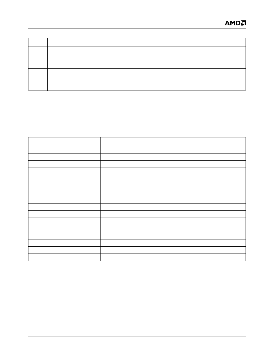
Table 6-55 illustrates the various frame buffer addressing schemes. In the table, MAx represents the frame buffer memory
address signals, Ax represents the CRTC address counter signals, RSx represents row scan counter output bits. The
binary value in the column headings is a concatenation of the DWORD Mode and Byte Mode bits. (i.e., {DWORD Mode,
ByteMode} in verilog.)
1
SL_RSCBT
Select Row Scan Bit. This bit determines which CRTC signal appears on the MA14
address bit sent to the frame buffer memory. If this bit is a 0, bit 1 of the Row Scan
counter appears on MA14. If this bit is a 1, then CRTC address counter bit 14, 13, or 12
appears on MA14. See Table 6-55 on page 371 for more information.
0
SL_A13
Select A13. This bit determines which CRTC signal appears on the MA13 address bit
sent to the frame buffer memory. If this bit is a 0, bit 0 of the Row Scan counter appears
on MA13. If this bit is a 1, then CRTC address counter bit 13, 12, or 11 appears on MA13.
See Table 6-55 on page 371 for more information.
Table 6-55. CRTC Memory Addressing Modes
Frame Buffer Memory Address Bit
Byte Mode (01)
Word Mode (00)
DWORD Mode (1X)
MA0
A0
A15 or A13
A12
MA1
A1
A0
A13
MA2
A2
A1
A0
MA3
A3
A2
A1
MA4
A4
A3
A2
MA5
A5
A4
A3
MA6
A6
A5
A4
MA7
A7
A6
A5
MA8
A8
A7
A6
MA9
A9
A8
A7
MA10
A10
A9
A8
MA11
A11
A10
A9
MA12
A12
A11
A10
MA13
A13 or RS0
A12 or RS0
A11 or RS0
MA14
A14 or RS1
A13 or RS1
A12 or RS1
MA15
A15
A14
A13
CRTC Mode Control Register Bit Descriptions (Continued)
Bit
Name
Description