6 display controller register descriptions, Display controller register descriptions, Table 6-45 – AMD Geode LX [email protected] User Manual
Page 300: Standard geodelink™ device msrs summary, Table 6-46, Dc specific msrs summary, Table 6-47, Dc configuration control register summary
300
AMD Geode™ LX Processors Data Book
Display Controller Register Descriptions
33234H
6.6
Display Controller Register Descriptions
This section provides information on the registers associ-
ated with the Display Controller (DC) (i.e., GUI and VGA
blocks), including the Standard GeodeLink™ Device (GLD)
MSRs and the Display Controller Specific MSRs (accessed
via the RDMSR and WRMSR instructions). Table 6-45
through Table 6-50 are register summary tables that
include reset values and page references where the bit
descriptions are provided.
Note:
The MSR address is derived from the perspective
of the CPU Core. See Section 4.1 "MSR Set" on
page 45 for more details on MSR addressing.
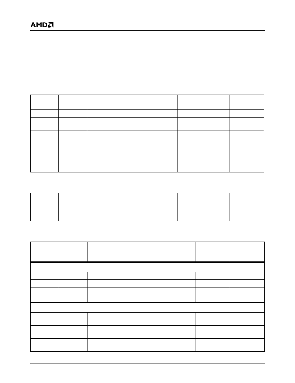
Table 6-45. Standard GeodeLink™ Device MSRs Summary
MSR
Address
Type
Register Name
Reset Value
Reference
80002000h
RO
GLD Capabilities MSR (GLD_MSR_CAP)
00000000_0003E4xxh
80002001h
R/W
GLD Master Configuration MSR
(GLD_MSR_CONFIG)
00000000_00000000h
80002002h
R/W
GLIU0 Device SMI MSR (GLD_MSR_SMI)
00000000_00000000h
80002003h
R/W
00000000_00000000h
80002004h
R/W
GLD Power Management MSR
(GLD_MSR_PM)
00000000_00000015h
80002005h
R/W
GLIU0 Device Diagnostic MSR
(GLD_MSR_DIAG)
00000000_00000000h
Table 6-46. DC Specific MSRs Summary
MSR
Address
Type
Register Name
Reset Value
Reference
80000012h
R/W
DC RAM Control MSR
(DC_RAM_CTL_MSR)
00000000_02020202h
Table 6-47. DC Configuration Control Register Summary
DC
Memory
Offset
Type
Register Name
Reset Value
Reference
Configuration and Status Registers
000h
R/W
00000000h
004h
R/W
DC General Configuration (DC_GENERAL_CFG)
00000000h
DC Display Configuration (DC_DISPLAY_CFG)
00Ch
R/W
DC Arbitration Configuration (DC_ARB_CFG)
00000000h
Memory Organization Registers
010h
R/W
DC Frame Buffer Start Address
(DC_FB_ST_OFFSET)
xxxxxxxxh
014h
R/W
DC Compression Buffer Start Address
(DC_CB_ST_OFFSET)
xxxxxxxxh
018h
R/W
DC Cursor Buffer Start Address
(DC_CURS_ST_OFFSET)
xxxxxxxxh