Figure 7-4, Power up sequencing, Figure 7-5 – AMD Geode LX [email protected] User Manual
Page 609: Table 7-9, Pci interface signals
AMD Geode™ LX Processors Data Book
609
Electrical Specifications
33234H
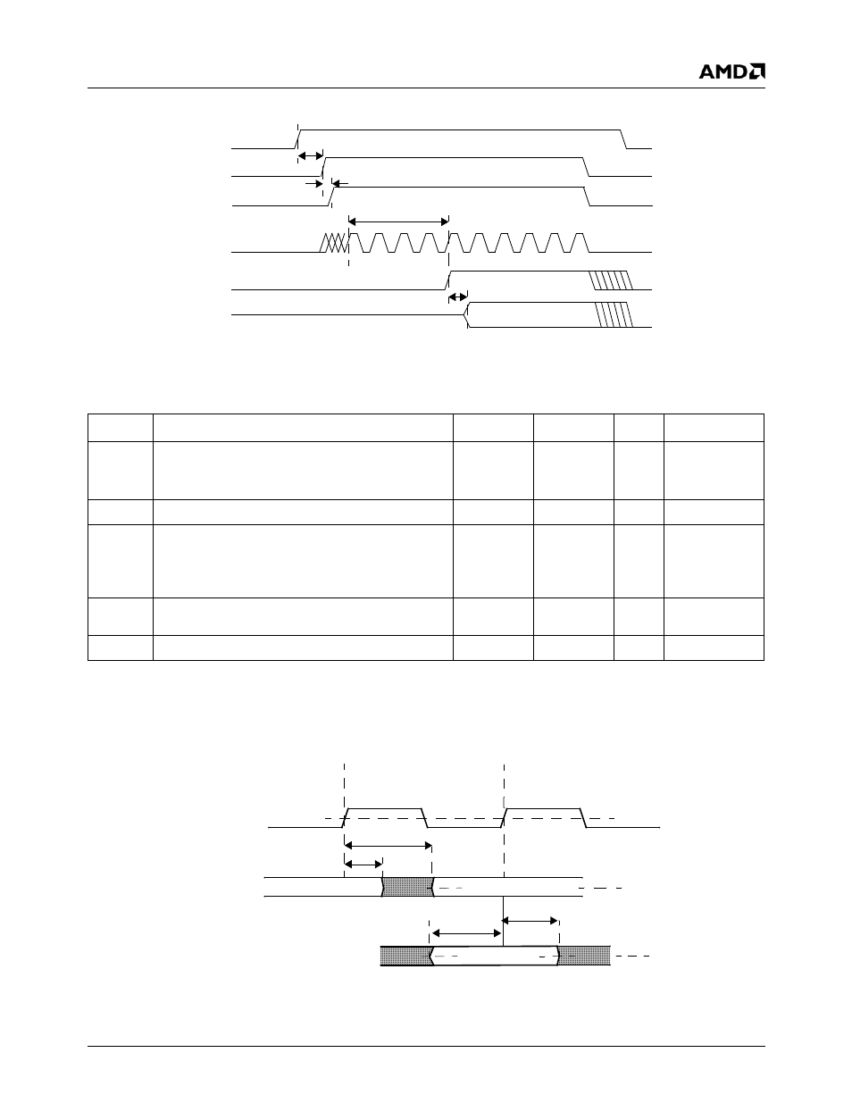
Figure 7-4. Power Up Sequencing
Figure 7-5. Drive Level and Measurement Points for Switching Characteristics
V
CORE
V
IO
,V
MEM
RESET#
SYSREF
SYSREF
cycle time not
to scale with
other delays
in this figure.
Outputs
t
ON
t
RSTX
t
Z
MVREF
t
MVON
Table 7-9. PCI Interface Signals
Symbol
Parameter
Min
Max
Unit
Comments
t
SU1
Input Setup time to SYSREF
(AD[31:0], DEVSEL#,GNT[2:0]#, IRDY#, PAR,
STOP#, TRDY#)
3.0
ns
t
SU2
REQ[2:0]# Input Setup time to SYSREF
4.5
ns
t
H
Input Hold time from SYSREF for all PCI inputs
(STOP#)
(DEVSEL#, FRAME#, GNT[2:0#, IRDY#, PAR,
TRDY#, REQ[2:0]#, STOP#)
0
ns
Note 1
t
VAL1
Bused signals Valid Delay time from SYSREF
(AD[31:0])
2.0
6.0
ns
Note 2
t
VAL2
GNT[2:0]# Valid Delay time from SYSREF
2.0
5.5
ns
Note 1. The GNT[2:0]#, IRQ13, SUSPA#, PW0, and PW1 signals are only inputs during RESET# active. They must be sta-
ble between five and two PCI clocks before RESET# inactive.
Note 2. Output delay includes tristate-to-valid transitions and valid-to-tristate timing.
SYSREF
Outputs
Inputs
50%
Valid Input
Valid Output
n+1
Valid Output
n
50%
50%
t
VAL1,2
Min
t
VAL1,2
Max
t
SU1,2
t
H1,2