Table 5-7, Cr4 bit descriptions, Table 5-8 – AMD Geode LX [email protected] User Manual
Page 96: Cr3 bit descriptions, Table 5-9, Cr2 bit descriptions, Table 5-10, Cr0 bit descriptions
96
AMD Geode™ LX Processors Data Book
CPU Core
33234H
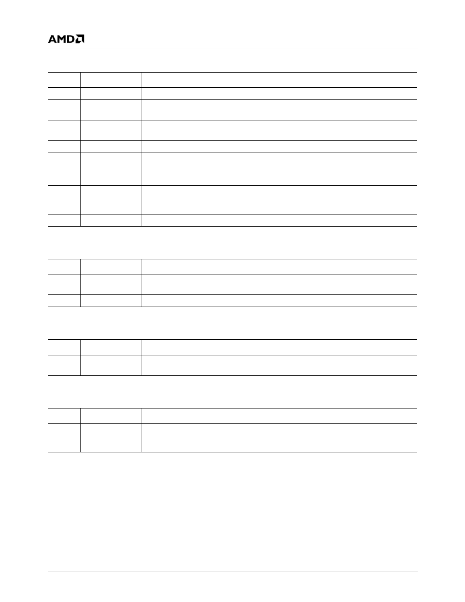
Table 5-7. CR4 Bit Descriptions
Bit
Name
Description
31:9
RSVD
Reserved. Set to 0 (always returns 0 when read).
8
PCE
Performance Counter Enable. Set PCE = 1 to make RDPMC available at nonzero privi-
lege levels.
7
PGE
Page Global Enable. Set PGE = 1 to make global pages immune to INVLPG instruc-
tions.
6:5
RSVD
Reserved. Set to 0 (always returns 0 when read).
4
PSE
Page Size Extensions. Set PSE = 1 to enable 4 MB pages.
3
DE
Debug Extensions. Set DE = 1 to enable debug extensions (i.e., DR4, DR5, and I/O
breakpoints).
2
TSC
Time Stamp Counter Instruction.
0: RDTSC instruction enabled for all CPL states.
1: RDTSC instruction enabled for CPL = 0 only.
1:0
RSVD
Reserved. Set to 0 (always returns 0 when read).
Table 5-8. CR3 Bit Descriptions
Bit
Name
Description
31:12
PDBR
Page Directory Base Register. Identifies page directory base address on a 4 KB page
boundary.
11:0
RSVD
Reserved. Set to 0.
Table 5-9. CR2 Bit Descriptions
Bit
Name
Description
31:0
PFLA
Page Fault Linear Address. With paging enabled and after a page fault, PFLA contains
the linear address of the address that caused the page fault.
Table 5-10. CR0 Bit Descriptions
Bit
Name
Description
31
PG
Paging Enable Bit. If PG = 1 and protected mode is enabled (PE = 1), paging is
enabled. After changing the state of PG, software must execute an unconditional branch
instruction (e.g., JMP, CALL) to have the change take effect.