3 memory interface signals (ddr) – AMD Geode LX [email protected] User Manual
Page 35
AMD Geode™ LX Processors Data Book
35
33234H
3.4.3
Memory Interface Signals (DDR)
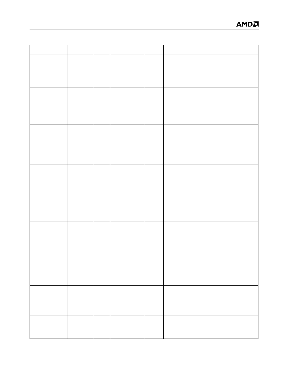
Signal Name
Ball No.
Type
f
V
Description
SDCLK[5:0]P,
SDCLK[5:0]N
D20, D21,
D23, D24,
J28, H28,
M28, L28,
J4, H4,
M4, L4
O
up to 200 MHz
2.5
SDRAM Clock Differential Pairs. The SDRAM
devices sample all the control, address, and
data based on these clocks. All clocks are dif-
ferential clock outputs.
MVREF
P1
I
Analog
V
MEM
Memory Voltage Reference. This input oper-
ates at half the V
MEM
voltage.
CKE[1:0]
F4, E4
I/O
up to 200 Mb/s
2.5
Clock Enable. For normal operation, CKE is
held high. CKE goes low during Suspend.
CKE0 is used with CS0# and CS1#. CKE1 is
used with CS2# and CS3#.
CS[3:0]#
D30, F29,
F28, B28
I/O
up to 200 Mb/s
2.5
Chip Selects. The chip selects are used to
select the module bank within the system mem-
ory. Each chip select corresponds to a specific
module bank.
If CS# is high, the bank(s) do not respond to
RAS#, CAS#, or WE# until the bank is selected
again.
RAS[1:0]#
D27, C26
I/O
up to 200 Mb/s
2.5
Row Address Strobe. RAS#, CAS#, WE#, and
CKE are encoded to support the different
SDRAM commands. RAS0# is used with CS0#
and CS1#. RAS1# is used with CS2# and
CS3#.
CAS[1:0]#
E29, E28
I/O
up to 200 Mb/s
2.5
Column Address Strobe. RAS#, CAS#, WE#,
and CKE are encoded to support the different
SDRAM commands. CAS0# is used with CS0#
and CS1#. CAS1# is used with CS2# and
CS3#.
WE[1:0]#
A28, C27
I/O
up to 200 Mb/s
2.5
Write Enable. RAS#, CAS#, WE#, and CKE
are encoded to support the different SDRAM
commands. WE0# is used with CS0# and
CS1#. WE1# is used with CS2# and CS3#.
BA[1:0]
C20, D26
I/O
up to 200 Mb/s
2.5
Bank Address Bits. These bits are used to
select the component bank within the SDRAM.
MA[13:0]
See Table
I/O
up to 200 Mb/s
2.5
Memory Address Bus. The multiplexed row/
column address lines driven to the system
memory.
Supports 256-Mbit SDRAM.
TLA[1:0]
B13, B15
I/O
up to 200 Mb/s
2.5
Memory Debug Pins. These pins provide use-
ful memory interface debug timing signals.
(Should be wired to DIMM slot.)
TLA[0] is wired to DQS[8] on the DIMM
TLA[1] is wired to CB[0] on the DIMM
DQS[7:0]
N31, J29,
B23, C19,
A10, C6,
H3, M2
I/O
up to 200 MHz
2.5
DDR Data Strobe.