13 vip task a v offset (vip_task_a_v_offset), Vip task a v offset (vip_task_a_v_offset), 00000000h – AMD Geode LX [email protected] User Manual
Page 499
AMD Geode™ LX Processors Data Book
499
Video Input Port Register Descriptions
33234H
6.10.2.13 VIP Task A V Offset (VIP_TASK_A_V_OFFSET)
7
EFD
Even Field UV Decimation. When set to 1, the U and V values of the even frame will be
discarded.
Note:
The DD bit (VIP Memory Offset 00h[16]) should be set to 1 or even lines will also
be decimated.
6
TP
Task Polarity. When set to 1, the input TASK bit is inverted.
5
VP
VSYNC Polarity. This bit is set to 1 when the VSYNC input is active high (high during
VBLANK) or 0 when the VSYNC input is active low (low during VBLANK). This is only
used for 601 type input video where HSYNC and VSYNC signals are used rather then
the SAV/EAV codes.
4
HP
HSYNC Polarity. This bit is set to 1 when the HSYNC input is active high (high during
HBLANK) or 0 when the HSYNC input is active low (low during HBLANK). This is only
used for 601 type input video where HSYNC and VSYNC signals are used rather then
the SAV/EAV codes.
3:1
RSVD
Reserved.
0
FR
FIFO Reset. Setting this bit forces the VIP FIFO pointers and data counts to their reset
state. This might be used in cases where high GLIU latencies cause continuous FIFO
overflows, when a line overrun error occurs, or if the line offset gets corrupted which
could result in an image shift. This bit remains a 1 during the FIFO reset sequence. When
the FIFO reset sequence has completed, this bit is automatically reset to a 0.
The FIFO reset sequence consists of:
Input reception is halted.
The input and output FIFO addresses and data counts are reset.
Wait for all outstanding GLIU requests to be completed.
The FIFO Reset bit is set to 0.
Input data reception starts after the programmed run control event has occurred (i.e.,
start of line, field, frame).
VIP Memory Offset 30h
Type
R/W
Reset Value
00000000h
VIP_CONTRL_REG3 Bit Descriptions (Continued)
Bit
Name
Description
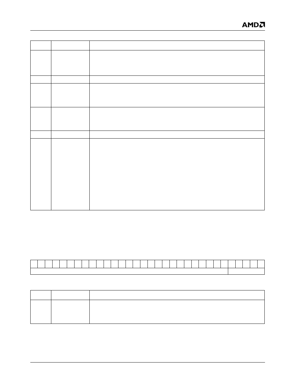
VIP_TASK_A_V_OFFSET Register Map
31 30 29 28 27 26 25 24 23 22 21 20 19 18 17 16 15 14 13 12 11 10
9
8
7
6
5
4
3
2
1
0
TASK_A_V_ODD_OFFSET
Program to 00000
VIP_TASK_A_V_OFFSET Bit Descriptions
Bit
Name
Description
31:0
TASK_A_V_
ODD_OFFSET
Task A V Odd Offset. This register determines the starting address of the V buffer when
data is stored in planar format. The start of the V buffer is determined by adding the con-
tents of this register to that of the base address. This value must be 32-byte aligned. (Bits
[4:0] are required to be 00000.)