4 dc compression fifo diagnostic (dc_cfifo_diag), Dc compression fifo diagnostic (dc_cfifo_diag) – AMD Geode LX [email protected] User Manual
Page 337
AMD Geode™ LX Processors Data Book
337
Display Controller Register Descriptions
33234H
6.6.7.4
DC Compression FIFO Diagnostic (DC_CFIFO_DIAG)
This register is provided to enable testability of the compressed line buffer (FIFO) RAM. Before it is accessed, the DIAG bit
should be set high (DC Memory Offset 004h[28] = 1) and the DFLE bit should be set low (DC Memory Offset 004h[0] = 0).
Also, the CFRW bit in DC_GENERAL_CFG (DC Memory Offset 004h[29]) should be set appropriately depending on
whether a series of reads or writes is to be performed. After each write, the FIFO write pointer automatically increments.
After all write operations are performed, the CFRW bit should be set high to enable read addresses to the FIFO and a pair
of reads of don't care data should be performed to load 64 bits of data into the output latch. Each subsequent read contains
the appropriate data that was previously written. After each pair of reads, the FIFO read pointer automatically increments.
DC Memory Offset 07Ch
Type
R/W
Reset Value
xxxxxxxxh
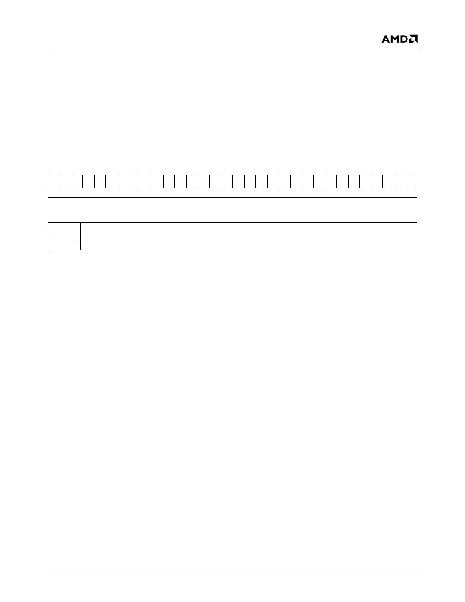
DC_CFIFO_DIAG Register Map
31 30 29 28 27 26 25 24 23 22 21 20 19 18 17 16 15 14 13 12 11 10
9
8
7
6
5
4
3
2
1
0
CFIFO_DATA
DC_CFIFO_DIAG Bit Descriptions
Bit
Name
Description
31:0
CFIFO_DATA
Compressed Data FIFO Diagnostic Read or Write Data.