Table 7-16, Jtag interface signals – AMD Geode LX [email protected] User Manual
Page 617
AMD Geode™ LX Processors Data Book
617
Electrical Specifications
33234H
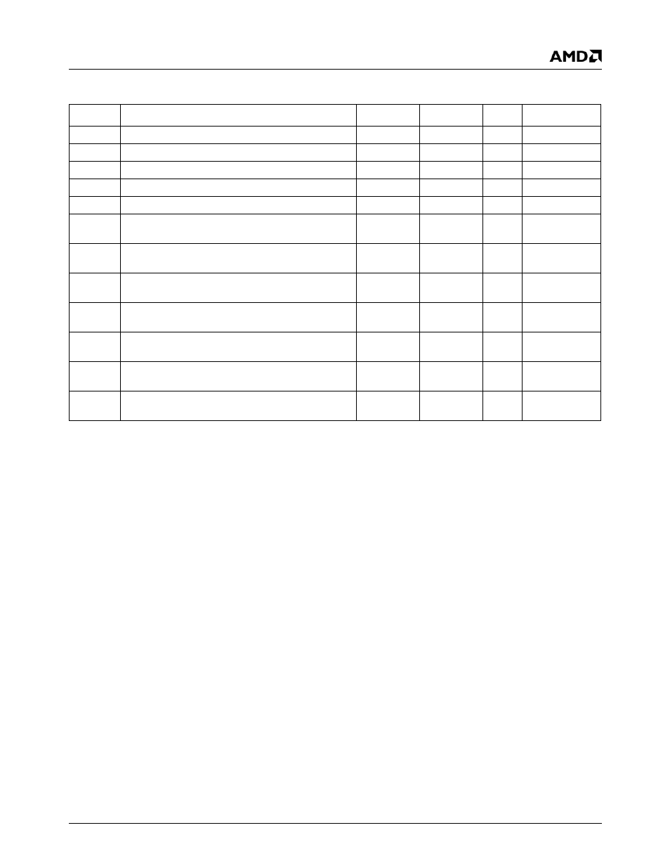
Table 7-16. JTAG Interface Signals
Symbol
Parameter
Min
Max
Unit
Comments
TCLK period
15
ns
Note 1
TCLK High time
4
ns
40% period
TCLK Low time
4
ns
40% period
TDI, TMS Setup time to TCLK rising edge
1.5
ns
TMS Hold time from TCLK rising edge
3.0
ns
TDI Hold time from TCLK rising edge - Boundary
scan
3.0
ns
TDI Hold time from TCLK rising edge - Functional
2*T
GLBus
ns
Hold for 2
GLBus clocks
TDO Output Valid Delay time from TCLK falling
edge when running boundary scan test
3.0
70.0
ns
TDO Output Valid Delay time from TCLK falling
edge in normal functional mode
3.0
10.0
ns
All chip I/O Setup time to TCLK rise - boundary
scan
1.0
ns
All chip I/O Hold time from TCLK rise - boundary
scan
3
ns
All chip I/O Output Valid Delay time from TCLK
falling edge - boundary scan test
2.0
70.0
ns
Note 1. TCLK limited during functional mode to 100 MHz or 1/4 of the memory data frequency.